Continue to Site

Welcome to EDAboard.com

Welcome to our site! EDAboard.com is an international Electronics Discussion Forum focused on EDA software, circuits, schematics, books, theory, papers, asic, pld, 8051, DSP, Network, RF, Analog Design, PCB, Service Manuals... and a whole lot more! To participate you need to register. Registration is free. Click here to register now.

IXFX180N25T Mosfet Burn

Status
Not open for further replies.

Vishal_thomas

Newbie level 4
Joined
May 27, 2019
Messages
7
Helped
0
Reputation
0
Reaction score
0
Trophy points
1
Activity points
60
Hai,

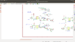
I am using IXFX180N25T mosfet for motor controller. Driving 8 mosfets in parallel in each leg with Infenion gate driver followed by current booster using transistor totem pole configuration. I used a series gate resistor of 1ohm for each individual mosfet after current Booster circuit. Each mosfet has 10K pull down and ceramic cap of 10nf at Gate-source.V/f algorithm with base rpm set to 3000 and max bus voltage 72V. Every time one mosfet of high side leg is getting burned, i have provided dead band of 5microsec.
The circuit is mounted on heat sink.I can see some unwanted triggering happening in mosfet because phase output is very high than expected.
The whole circuits works fine when am using infenion AUIRFP4568.

Kindly let me know any suggestions.
 

Hi,

Instead of description with words --> show your schematic.

I can see some unwanted triggering happening in mosfet because phase output is very high than expected.
What does this mean? Show scope pictures or hand drawn sketch of signals with volatge and timing infromation.

Klaus
 

scope_19.png


The image Yellow is High side mosfet Vds and Green is low side mosfet Vds. does this means there is a cross conduction happening?
 

at the bottom of first page of
https://www.infineon.com/dgdl/para.pdf?fileId=5546d462533600a401535744b4583f79

"Unlike other switches4, parallel MOSFETs do not require additional sharing resistors, dynamic currentbalancing transformers or active feedback to the driver. It is demonstrated that MOSFET generated unbalance can beheld to acceptable levels through appropriate driver design or power circuit design or parameter screening. The degreeof control necessary is a function of the application."

the 4 after switches is a footnote indicator
 

IMG_20190523_204141.jpg
This is High side and low side Gate pulses. There clearly 5us dead time is visible. Why this effect is not visible on Vds voltages?
 

Attachments

  • Screenshot from 2019-05-27 18-27-13.png
    Screenshot from 2019-05-27 18-27-13.png
    108.1 KB · Views: 93

IMG_20190523_201232.jpg
yellow is high side Gate and Green low side gate pulse. Here the deadband is properly visible.
But when i checked Vds of high side and low side mosfets there is a overlap of signals.

scope_17.png
Yellow is High side Vds and green low side vds.
According to mosfet characteristics whether there is cross conduction happening for 50ns?
 

Hi,

Please make your schematic and description unambiguous.
I just checked "1 ohm" and "10 nF" ... but none does match your schematic. I didin´t check completely.

And please don´t post a lot of single informations. Combine them to one complete post.

This is High side and low side Gate pulses. There clearly 5us dead time is visible. Why this effect is not visible on Vds voltages?
What do you expect?
During dead time both transistors are OFF, the node is floating ... thus the voltage during dead time is not predictable. (wihtout load information)

Klaus
 

Okay sorry about that.
My gate resistors are;
1 ohm series with 8 paralleled 3.3ohms for each mosfet for TURN ON and 0ohm series with 8 paralled 3.3 ohms for TURN OFF.
In above schematic instead of 10nf capacitor initially i connected 15V tvs diode which was working fine with Infienion mosfet.
Later since new IXYS mosfet were Burning,i tried connecting 10nf capacitor,but it doesnt help.
 

Hi,

I´m now even more confused.

Klaus
 

Every circuit description you have given so far is partly contradicting the other. E.g. your latest posts tells about separate turn-on and turn-off resistors for each MOSFET, but that's impossible with the right schematic in post #4. Answering the simple question how is each MOSFET connected to gate driver(s), doe you have one or multiple drivers per bridge leg is just impossible.

Dedicated gate-source capacitors may be useful in some cases, but 10 nF is a huge value and probably increasing switching losses at lot. You didn't yet gave a motivation for it.

Also unclear is the bridge ouput wiring, cut in the post #4 schematic.
 

Screenshot from 2019-05-28 14-22-04.pngScreenshot from 2019-05-28 14-22-58.png

Sorry for the confusion.
Capacitor value i chose from the reference design Toshiba.
Does adding snubber for each individual Mosfet helps or just One for a leg is fine?
I found Sevcon Motor controller teardown photo,there they have r&c for each mosfet,whether it is a RC filter for gate pulse or RC snubber VDS?


Now i have Increased Turn On resistance to slow down the turning On. I hope it will help in preventing Cross conduction.
 

Status
Not open for further replies.

Similar threads

Part and Inventory Search

Welcome to EDABoard.com

Sponsor

Back
Top