Continue to Site

Welcome to EDAboard.com

Welcome to our site! EDAboard.com is an international Electronics Discussion Forum focused on EDA software, circuits, schematics, books, theory, papers, asic, pld, 8051, DSP, Network, RF, Analog Design, PCB, Service Manuals... and a whole lot more! To participate you need to register. Registration is free. Click here to register now.

Distance between poly gates in the matched array is different

Status
Not open for further replies.

Junus2012

Advanced Member level 5
Joined
Jan 9, 2012
Messages
1,552
Helped
47
Reputation
98
Reaction score
53
Trophy points
1,328
Location
Italy
Activity points
15,235
Dear friends,

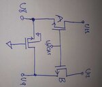
attached you see please my matched array for the given circuit.

As you can see that in the first array management every transistor was individual and the distance are identical between every gate.
In the second arrangement I merged the shared region to reduce the size of the layout, but as you see that distance are not becoming identical between each transistor in the array.

I don't know if that will effect the matching or not, but I have a feeling that the electrical characteristics of both might be different,

which one should be better ?

Thank you very much matched_array.jpeg
 

Well, in the second arrangement you have two A transistors that are merged and two B transistors, also merged. So, this kind of makes the two rows in this arrangement kind of the same. However, if I have to choose, I'll vote for the first arrangement because there all transistors are under same conditions (provided dummies are used on the sides).
 
Dear Suta,

As you said in the first arranegement with dummy transistors it will be fully symetrical circuiit. while in the second array the internel transistors will be etched differently from the outer een if there are dummuie.

But Suta if I have a bigger arrray of more than two transistor, suppose like ABCD, do you think that if the arrangement led to merge only A and B but not C and D ? soon I will provide you wit such connection to make the case more clear
 

There is also another possibility. Your transistors above as per the schematic don't have common nodes besides the gates. So, at a first glance you can't put them in the same diffusion. However, you can still use same diffusion area for both if you allow for a dummy that is connected across the two branches with gate to gnd - say one terminal of the dummy is connected to the left branch, the other to the right branch and gate to gnd. This way it will separate the transistors that are in the two branches but will give the possibility to use one contiguous diffusion area.
 
Dear Suta,

thank you for this smart idea, I see it is the best to implement, I have plot the circuit connection to be confirmed from you.. the only one thing I didn't simulate this topology so I don't know its impact yet on the circuit performance

Thank you once again

New Doc 62_2.jpg

New Doc 62_1.jpg
 

Attachments

  • New Doc 62_2.jpg
    New Doc 62_2.jpg
    223.5 KB · Views: 136

Thank you Suta,

I will try to simulate it then I give you a feedback
 

Status
Not open for further replies.

Part and Inventory Search

Welcome to EDABoard.com

Sponsor

Back
Top