Continue to Site

Welcome to EDAboard.com

Welcome to our site! EDAboard.com is an international Electronics Discussion Forum focused on EDA software, circuits, schematics, books, theory, papers, asic, pld, 8051, DSP, Network, RF, Analog Design, PCB, Service Manuals... and a whole lot more! To participate you need to register. Registration is free. Click here to register now.

[SOLVED] Solder dots on PCB traces

Status
Not open for further replies.

Milhouse11

Newbie level 2
Joined
May 24, 2019
Messages
2
Helped
0
Reputation
0
Reaction score
0
Trophy points
1
Activity points
19
Hi guys,

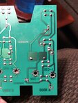
I’m wanting to redo a small circuit board for a garage door opener controller to work with an older opener. It should be pretty basic but I have no idea what these small dots of solder (circled in red) are along the traces of the PCB. They aren’t connected to anything on the other side of the board.

Any thoughts what they could be?
1B1B1F78-004D-4AB6-84ED-62BA8AF1CA00.jpg
 

We can’t predict but possibilities for multilayer PCB with buried vias or If it is a single layer PCB solder mask opened for test pints or wire connection
 

Hi,

I'm with Easy peasy: Test points.
And I assume this is no multilayer..I rather assume this is a cheap single side PCB.

Klaus
 
I would say test points too. Typically a board like that would be tested on a "bed of nails", a fixed platform with locating pins to align the board and spring loaded test probes to touch those solder dots. The probes would have wires going to test equipment. An operator would place the board on the pins and lock it down so pressure was applied to the probes then the tester would inject or measure signals at the probes to check functionality. It's a quick way to connect lots of test equipment without having to attach wires. Probing on component legs is normally avoided as the probe pressure could influence a poor solder joint and hide it.

Brian.
 
maybe things have changed in 20 - 25 years
i used to work for a company that used a bed of nails where the "nails" lined up
with the pins of all the components. the machine checked impedances with the goal
of finding incorrect values and components inserted incorrectly.
 

Awesome, thanks everyone for your replies.
 

Status
Not open for further replies.

Part and Inventory Search

Welcome to EDABoard.com

Sponsor

Back
Top