Continue to Site

Welcome to EDAboard.com

Welcome to our site! EDAboard.com is an international Electronics Discussion Forum focused on EDA software, circuits, schematics, books, theory, papers, asic, pld, 8051, DSP, Network, RF, Analog Design, PCB, Service Manuals... and a whole lot more! To participate you need to register. Registration is free. Click here to register now.

What does this resistor do in MOS differential pair, and how it's implemented

Status
Not open for further replies.

alfhg

Newbie level 2
Joined
May 11, 2019
Messages
2
Helped
0
Reputation
0
Reaction score
0
Trophy points
1
Activity points
18
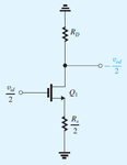
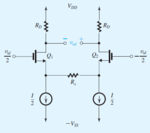
From Sedra & Smith, there is an NMOS differential pair in Fig.1, with a resistor Rs connected between the sources.

1. What's the effect of this resistor Rs?

I think its small signal, differential "half circuit" should be Fig.2. So its effects should be improving linearity by reducing Vgs, higher bandwidth, at the price of lower differential gain?

Are there any additional effects of Rs?

2. It also follows, Rs can be implemented using 2 FETs, as in Fig.3.
Are Q3 & Q4 NMOS or PMOS?
How does this circuit work, in both differential and common mode perspectives?
(As far as I can see, Q3 & Q4 do nothing in common mode, because the sources of Q1 & Q2 are at equal common mode voltage, so Q3 & Q4 are not conducting common mode currents.)

Thanks!
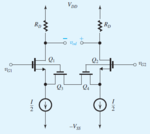
Fig3.png
Fig2.png
Fig1.png
 

It is a slew rate enhancement trick, at least that's what
I was told by peers; however I never saw anything much
from trying it in my op amp, comparator design efforts.

Splitting the tail into two pieces adds another mismatch
term.
 

1. Commonly understood term for the topology is source degeneration. I agree with your description of its purpose.
2. Obviously NMOS if we presume enhancement mode for Q1 - Q4. The circuit doesn't work much different than the resistor variant. Q3/Q4 can be expected to operate in triode region. Neither Rs nor Q3/Q4 are conducting common currents.
 
  • Like
Reactions: alfhg

    alfhg

    Points: 2
    Helpful Answer Positive Rating
It is a slew rate enhancement trick, at least that's what
I was told by peers; however I never saw anything much
from trying it in my op amp, comparator design efforts.

term.

May I ask how the slew rate improvement is achieved?
 

I think the version with Q3/4 also tries to avoid the non-linearity caused by the degeneration resistors because in a way they work with more or less constant Vgs (to a certain extend) and the resistance value is not modulated by the changing Vgs in the case when the gates are connected to a fixed voltage.
This circuit is not so much used as full blown diff pair as in the design of OTAs but rather as a gm cell, maybe used in Gm-C filters. The two separate tail currents apart from being a source of mismatch and offset also cause more noise at the output. Also, caps at the source of the diff pair transistors, together with the degeneration transistors form a zero which is in addition to the output poles. Maybe a good thing if they can cancel each other. Not always possible and in filter designs can be a headache.
Because of degeneration, we get higher output resistance. This is a good effect in Gm-C filter design because it makes the gm cell (together with its filter capacitances) look more like a real integrator.
As for the slewing, the cell goes into slewing not as easy as a regular diff pair. Again because of the degeneration - the gm is smaller than in the normal diff pair and it needs more input voltage difference to get saturated and start slewing.
 
Last edited:

Status
Not open for further replies.

Part and Inventory Search

Welcome to EDABoard.com

Sponsor

Back
Top