Continue to Site

Welcome to EDAboard.com

Welcome to our site! EDAboard.com is an international Electronics Discussion Forum focused on EDA software, circuits, schematics, books, theory, papers, asic, pld, 8051, DSP, Network, RF, Analog Design, PCB, Service Manuals... and a whole lot more! To participate you need to register. Registration is free. Click here to register now.

How does feedback loop control the duty cycle of buck regulator

Status
Not open for further replies.

sushl

Junior Member level 2
Joined
Aug 22, 2018
Messages
24
Helped
0
Reputation
0
Reaction score
0
Trophy points
1
Activity points
238
Hi All,

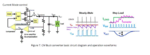
While going through internal structure of a buck regulator, there was a feedback loop connected from the voltage divider circuit therein connected to a comparator and the input fed to the SR flipflop R end. How does this feedback control the duty cycle ?
 

There are different topologies involving a comparator, current mode, voltage mode ore hysteretic. Please give more details.
 

The buck converter does not absolutely need a pulse generator to maintain its operation. The comparator (a) turns on when it senses a drop in output voltage, then (b) turns off when sufficient juice has been admitted to raise the voltage.

The result is a pulse train which operates the buck converter. Voltage regulation is pretty much automatic with this method.

This method requires a certain amount of hysteresis, achieved by a resistive or capacitive network. The aim is to provide snap action. High gain is able to achieve this. A plain logic gate can do the job as well as the comparator and flip-flop.

I made a simulation where two transistors (as a sziklai pair) drive a buck converter.

A single transistor might be persuaded to oscillate if its gain is sufficiently high. However a condition can happen where it stays on constantly at some middle extent, operating as resistive drop instead of On-Off fashion.
 

There is typically a voltage to pwm conversion circuit of some sort.

A common one is a comparator that compares a ramp function to the error amplifier output.
 

Switch regulator feedback circuits may differ greatly in details, but they all function similarly:

If the output voltage is to high, they adjust the PWM duty-cycle to reduce the voltage.
If the output voltage is to low, they adjust the PWM duty-cycle to increase the voltage.
If the output voltage is just right, the the PWM duty-cycle is not changed.

You have to examine the circuit design to determine how that is done for a particular circuit.
Typically it's done with a comparator the has the error voltage as one input and a sawtooth fed to the other input.
 
Last edited:

Hi all Thanks for the replies;
please find the attachment,

the regulator is operated in current mode, it consists of an internal clock generator, error amplifier and current sense.
I have 2 questions

The error signal is compared with the current slope ramp signal and that is given to the reset input of the sr filpflop. why is this done?
Also why not connect the error signal directly to the reset input? (can this method also control the duty cycle?)

thanks and regards
sush
 

Attachments

  • current_Mode_control_buckreg.png
    current_Mode_control_buckreg.png
    122.1 KB · Views: 126
Last edited by a moderator:

The error signal is compared with the current slope ramp signal and that is given to the reset input of the sr filpflop. why is this done?
Don't know what you mean with "current slope ramp". The error signal is primarily compared with current measurement, the current measurement is optionally modified by slope compensation signal. To understand the working of this topology, start with the simple case without slope compensation. Then learn when slope compensation is necessary.

Also why not connect the error signal directly to the reset input? (can this method also control the duty cycle?)
Not properly. It can work as hysteretic controller as in 34064.
 
  • Like
Reactions: sushl

    sushl

    Points: 2
    Helpful Answer Positive Rating
...
the regulator is operated in current mode, it consists of an internal clock generator, error amplifier and current sense.
I have 2 questions

The error signal is compared with the current slope ramp signal and that is given to the reset input of the sr filpflop. why is this done?
Also why not connect the error signal directly to the reset input? (can this method also control the duty cycle?)

thanks and regards
sush

If the error signal is fed directly to reset input of the SR flip flop, then peak current limiting would not be achieved. Comparing the error signal with the measured current inferred voltage, allows for current limiting to be achieved. The error signal input of the comparator always have a maximum voltage of some sort that switches the pwm when the current sense voltage gets to that value.

The slope compensation signal is used in situations where duty cycle is greater than 50% to modify the slope of the current sense signal basically for effective control.

The pwm can still be controlled without current sense but you'll have to use the voltage mode control scheme.
 
  • Like
Reactions: sushl

    sushl

    Points: 2
    Helpful Answer Positive Rating
Hi,

Also why not connect the error signal directly to the reset input?
The "error" signal usually is an analog signal
The RS input is a digital signal

The comparator generates a digital signal by comparing two analog signals.

Klaus
 
  • Like
Reactions: sushl

    sushl

    Points: 2
    Helpful Answer Positive Rating
reset input of the sr filpflop. why is this done?

The separate functions are shown in the schematic, although it is possible for a device to combine functions.

The SR flip-flop is in one state or the other, never at a midway position. It clarifies that resistive drop is not at work here.
 

Status
Not open for further replies.

Similar threads

Part and Inventory Search

Welcome to EDABoard.com

Sponsor

Back
Top