abcx123
Newbie level 3
Hi,
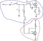
As my understanding on biasing circuit, it is used to provide stable and desired voltage level to the amplifier, so that the amplifier can be operated in desired region (eg. saturated region).
My question is that if I have an LNA with schematic as shown in the picture below, how is the biasing circuit for the inductive degeneration configuration NMOS constructed for Vbias1?

If a current mirror configuration biasing circuit (red square) is used, the sp (eg, S11, S21) will be affected.

In my opinion, they are affected because they are interpreted as part of input matching. Please correct me if I'm wrong. Is there any biasing circuit for LNA with Chebyshev bandpass filter instead of connecting directly to a power source?
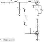
As my understanding on biasing circuit, it is used to provide stable and desired voltage level to the amplifier, so that the amplifier can be operated in desired region (eg. saturated region).
My question is that if I have an LNA with schematic as shown in the picture below, how is the biasing circuit for the inductive degeneration configuration NMOS constructed for Vbias1?
If a current mirror configuration biasing circuit (red square) is used, the sp (eg, S11, S21) will be affected.
In my opinion, they are affected because they are interpreted as part of input matching. Please correct me if I'm wrong. Is there any biasing circuit for LNA with Chebyshev bandpass filter instead of connecting directly to a power source?