tina.sax
Newbie level 1
Hi,
I am designing a PA.
I have two modules- Input and Output.
Input module is perfectly working with bypass capacitors and all stability networks. But in Output module, without bypass capacitors on drain bias, results are perfect. But, as I am putting bypass capacitor, after 2-3 iterations, job starts failing showing this error.
-------------------------------------------------------------------------------
Generating mesh at 4 GHz...
--- ERROR ---------------------------------------------------------------------
At least one port pin or bondwire end is not
fully connected to a conductive part of the
design (see the layout processing report for
details).
This setup is invalid for a Momentum simulation.
Same, bypass capacitors and hole drawing is done on Input side, its perfectly fine. Please provide the solution for debugging it.
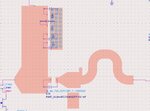
Figure is attached.
Thanks,
Tina
I am designing a PA.
I have two modules- Input and Output.
Input module is perfectly working with bypass capacitors and all stability networks. But in Output module, without bypass capacitors on drain bias, results are perfect. But, as I am putting bypass capacitor, after 2-3 iterations, job starts failing showing this error.
-------------------------------------------------------------------------------
Generating mesh at 4 GHz...
--- ERROR ---------------------------------------------------------------------
At least one port pin or bondwire end is not
fully connected to a conductive part of the
design (see the layout processing report for
details).
This setup is invalid for a Momentum simulation.
Same, bypass capacitors and hole drawing is done on Input side, its perfectly fine. Please provide the solution for debugging it.
Figure is attached.
Thanks,
Tina