Continue to Site

Welcome to EDAboard.com

Welcome to our site! EDAboard.com is an international Electronics Discussion Forum focused on EDA software, circuits, schematics, books, theory, papers, asic, pld, 8051, DSP, Network, RF, Analog Design, PCB, Service Manuals... and a whole lot more! To participate you need to register. Registration is free. Click here to register now.

common source pole calculation vs. simulation

Status
Not open for further replies.

daniel442

Junior Member level 2
Joined
Dec 29, 2017
Messages
20
Helped
0
Reputation
0
Reaction score
0
Trophy points
1
Activity points
199
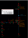
I would like to compare my pole simulation results to my hand calculations, I'm receiving quite a big error. when simulating a Common Source stage without output capacitance load there is a big difference between the simulated and the calculated poles, when I'm adding a capacitor load the output pole is similar but the input (which didn't change) is not... maybe I didn't model the MOSFET correctly?
calc.pngpole_w_load.pngpole_wo_load.png
 

What you are assuming, or the ground of hand calculation is simply RC based on the extracted DC. But the AC model of a particular technology is much complicated BSIM based model and could lead up to 300+ parameters. However there should be a near-match (may be 10%). Did you took Rout into account? may be its too low to change the math for such a small length?
 

yes, I've tried adding 1/gds in parallel - results didn't vary much...
 

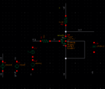
It seems there could be some issue on the method simulator follows to calculate the pole. I tried by myself and found a good match between hand calculation and simulator output. Here's using tsmc 180nm tech, I had to 'mimic' your TB. Therefore I used a bit more width than that of you.

sch1.PNG

and the preparation of TB with stimuli and declared variables-

adel.PNG

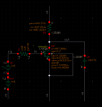
Here I did basic DC analysis and the AC to check the poles, Here's the DC results-

sch2.PNG
op_details.PNG

As you can see the gm is about 1.31m, output impedance of (1k||14.5k) sets a dc gain of 1.7 dB.
As the gate Cap is quite low for this size, around 4fF, with used Ri = 100, it gives a input pole of 398 GHz. Besides the sim says-

input_pole.PNG

Notice that there is no drop through input Ri, hence the dc gain in this input node is 0 dB.

As the load is 1pF, the other cap on this node 'quite' ignoble for handcalc, with output impedance = 0.95k, it gives a input pole of 168 MHz. Besides the sim says-

output_pole.PNG\

Hope this helps!
 

As the gate Cap is quite low for this size, around 4fF
How did you calculate it as 4[fF] ? I calculated it as - Cgd(1+gmRd)+Cgs=1.9[fF] - assuming Miller's effect
 

How did you calculate it as 4[fF] ? I calculated it as - Cgd(1+gmRd)+Cgs=1.9[fF] - assuming Miller's effect

You don't need to calculate like that using textbook approach. the total calculated gate cap is termed as Cgg, (or Cgs), check the opamp parameters attached.
 

I would like to compare my pole simulation results to my hand calculations, I'm receiving quite a big error. when simulating a Common Source stage without output capacitance load there is a big difference between the simulated and the calculated poles, when I'm adding a capacitor load the output pole is similar but the input (which didn't change) is not... maybe I didn't model the MOSFET correctly?
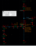
View attachment 152434View attachment 152435View attachment 152436

I think what the simulator gives you in the first schematic picture is ballpark correct and expected.

Your Cgg=3.9ff and the load cap is 10pF. Gain is gmR0 = 1.17, so there is not much Miller multiplication for Cgd. Your input resistor is only 100 Ohm and it sees a capacitor of about 4ff. At the same time your output pole is at much much lower frequency. So, by the time the input pole kicks in, your output is effectively ac shorted and thus there is no Miller effect. Approximate hand calculations show for the output pole 1/R0/C0 = 100e6 rad/s or 16MHz.
The input pole is 1/R3/Cgg = 1/(100*4ff) = 2.5e12 rad/s or approx 400GHz.
 

Thanks for the explanation, I understand the input pole now - Cgg is the total input capacitance.
for the output pole without Cout load, which capacitance should I take into consideration ? I have taken Cgd*MILLER_AMP (which equal 1.8) and Cdb and got an output pole of 112G instead of 66G...
 

I don't think it is going to be that easy if you don't have the load cap. You will have three time constants - for input cap Cgg, for Cgd and for the output cap which is at least Cjd. But the system is second order. Then, these time constants interact and since none of them really strongly dominates, it is difficult to separate the poles except you do more math.

BTW, to know more precisely the output cap in this case, probably it is better to just simulate it and see which of the values in the OP table matches better with the simulation.
 

Status
Not open for further replies.

Similar threads

Part and Inventory Search

Welcome to EDABoard.com

Sponsor

Back
Top