Continue to Site

Welcome to EDAboard.com

Welcome to our site! EDAboard.com is an international Electronics Discussion Forum focused on EDA software, circuits, schematics, books, theory, papers, asic, pld, 8051, DSP, Network, RF, Analog Design, PCB, Service Manuals... and a whole lot more! To participate you need to register. Registration is free. Click here to register now.

Deaign of low ON resistor CMOS transmission gate

Status
Not open for further replies.

Junus2012

Advanced Member level 5
Joined
Jan 9, 2012
Messages
1,552
Helped
47
Reputation
98
Reaction score
53
Trophy points
1,328
Location
Italy
Activity points
15,235
Dear all,

I am trying to design a CMOS TG with Ron = 10 Ohm maximum because I want to use it as an switch. But it is becoming difficult to reach this value and I need to increase the size of the MOS too much which leads to increase the parasitic capacitors and the switching time.

Do you think the 10 Ohm is not realistic or practical value for CMOS TG ? or these is other technique to reduce it further

Thank you
 

There are many IC products out there which beat this
Ron, and many CMOS muxes that don't (for the tradeoff
you note - low Ron = fat FETs and crosstalk / leakage sum).

Nothing for it, really, but to find the best trade (or a
better technology-node, but you've got a voltage limit
that tends to track Leff and thus Ron*W).

Getting away from "digital" devices could be a play,
look at silicide / salicide block features which are used
to form the Ldd (but add unwanted source and drain
resistances, for analog signals of less applied standoff
voltage).
 
It is very much dependent on technology. I can tell you, for example that the thick oxide option in 40nm technology requires something like 300/0.27 for the NMOS transistor at Vgs=1.2V to get close to Ron = 10 Ohm. In A TG this size will reduce but in any case it is a bulky transistor. Especially in 0.35nm technology which I think you are using.
 
No there is no other way, other than using MEMS switches.
If you are targeting ONLY a particular frequency, then you can bootstrap your source and gate through a large capacitor while isolating the gate through a large resistor. You can get a constant Vgs of Vdd which can reduce the size of your switch.
Else you can take a look at actively bootstrapped switches.. Check this link: https://www.seas.ucla.edu/brweb/papers/Journals/BRSummer15Switch.pdf
 
Dear Vivekroy
Dear Suta
Dear Freebird

Thank you all very much for your cooperation,

if I would go for tradional TG switch, then as Suta mentioned it is normal to expect big size transistor, for me I am using the 0.35 um technology. To get a Ron = 60 Ohm I am connecting NMOS with 80 um/ 0.35 um, the PMOS is three times bigger and so 240 um/ 0.35 um. I tried to make the PMOS equal to NMOS as many people like to do in digital world but that was giving me not stable resistor over range of voltage.

Now if I want to decrease the Ron I have to make the NMOS let say 120 um/0.35 um and then the PMOS 360 um/ 0.35... Do you think people are doing such big TG.


Dear Viveroky,

The switch MEMS will take more size than the TG gate I think. However I will keep it as an option. Indeed I proposed this solution to my supervisor 15 days ago but we dont have MEMS plus software to design it.

So now either I will use the classical TG or I will look for the solution you provided me in the link. I need to understand it before I can add more comment on it,

Thank you guys for your help
 

These are not "big" devices. If you look at RF switches
you will see mm of gate width (they need to have low
insertion loss in 50 ohm systems, often shoot for < 1ohm).

You want a CMOS transmission gate for DC and LF linearity.
For RF, the PMOS FET is just baggage and for linearity you
want a single FET, fully on (resistor) or fully off (capacitor,
and the parasitic caps had best be negligible - FDSOI FTW).
Such switches are often driven by a RC gate network with
a corner below spec min frequency so the gate travels with
the drain and source when "on" and at an offset when "off".
The LF corner (which impacts overall size, maybe more than
the active switch elements) also affects switching speed.

You should consider your application care-abouts in all of
this - if (for example) it's just a sampling switch feeding a
hold capacitor, do you care about linearity of on-resistance
at all (given signal range)? That's all the PMOS is there for,
passing current when the NMOS can't and making the
full range Ron - Vsource characteristic more of a bathtub
than a cliff.
 

There are different approaches to sizing the TG. All of them rely on square law behavior of the MOS transistor, which at 0.35u can still be a good assumption.
If you need a TG for a sampling switch that kind of compensates for charge injection - the NMOS and PMOS are with about the same size.
If you need TG either for sampling switch or just a general kind of switch, then people usually do PMOS about 3x bigger than NMOS. In any case, the TG on resistance will have a hump as you sweep the voltage across it. Size the ratio between P and N MOS such that you minimize the hump, that is make the ON resistance as flat as possible within the operating voltage range. This hump in the resistance will cause non-linearity. Then, size together the N and P MOS transistors to lower the TG resistance as per the needs.

You can use also the bootstrapped switch as was suggested, if your intended application allows for it. But have in mind that the bootstarpped switch is much more complicated circuit compared just with the TG.
 
Dear friends,

Thank you for your reply,

As I understood from Freebird that MOS size can reach mm width if I must have such low resistance value, it means for me if I design the PMOS with 400 um is still people can accept it its value.

from the reply from Suta,

I have looked to the bootstrap switch and seems it will complicate my design because I need many switches around my amplifier. Therefore as you kindly mentioned, I already simulated the TG and I noticed this hump and considering it as the worst case Ron. For sure the linearity is my concern as I am working with Analog circuit. I will follow your procedure to reduce this hump but this will change the ratio between the NMOS and the PMOS so it might be different than three ?

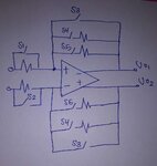
I will give you an idea aout my circuit, it is something like the one I attached below. The circuit provide configurable gain at frequency of 30 MHz. The worst case when I want to configure the amplifier as a buffer when closing S1, S2, S3... switches must have small resistance and high linearity for the entire range

conf.jpeg

Thank you once again
 

The worst case when I want to configure the amplifier as a buffer when closing S1, S2, S3...
I think you can design the on resistances of S1, S2, and S3 to be equal in this case. (i.e. Vo2/Vi2=-RS3/RS2)


Size the ratio between P and N MOS such that you minimize the hump, that is make the ON resistance as flat as possible within the operating voltage range.
I'd like your opinion on how industry designed switches are made. Some have very flat Ron and down to 10 ohms such as the ADG5412F.
https://www.analog.com/media/en/technical-documentation/data-sheets/adg5412f_5413f.pdf
Feel free not to answer if there are NDAs involved.
 

I have looked to the bootstrap switch and seems it will complicate my design because I need many switches around my amplifier. Therefore as you kindly mentioned, I already simulated the TG and I noticed this hump and considering it as the worst case Ron. For sure the linearity is my concern as I am working with Analog circuit. I will follow your procedure to reduce this hump but this will change the ratio between the NMOS and the PMOS so it might be different than three ?
You should try to minimize the resistance variation across your voltage range of operation, else indeed you will get poor linearity. For that if the ratio needs to be different than 3, so be it. And you can tune the value of your resistors to meet the gain values you want in presence of a larger switch resistance.

- - - Updated - - -

I'd like your opinion on how industry designed switches are made. Some have very flat Ron and down to 10 ohms such as the ADG5412F.
https://www.analog.com/media/en/technical-documentation/data-sheets/adg5412f_5413f.pdf
Feel free not to answer if there are NDAs involved.

It is heavily process dependent unfortunately! People often select a process technology based on where they get the best performance of a switch in very critical programmable RF applications.
 
Dear friends,


I have looked to the bootstrap switch and seems it will complicate my design because I need many switches around my amplifier. Therefore as you kindly mentioned, I already simulated the TG and I noticed this hump and considering it as the worst case Ron. For sure the linearity is my concern as I am working with Analog circuit. I will follow your procedure to reduce this hump but this will change the ratio between the NMOS and the PMOS so it might be different than three ?

The ratio of 3 is not cast in stone. It is just a rule of thumb. But you can change to whatever works for you.

- - - Updated - - -

I'd like your opinion on how industry designed switches are made. Some have very flat Ron and down to 10 ohms such as the ADG5412F.
https://www.analog.com/media/en/technical-documentation/data-sheets/adg5412f_5413f.pdf
Feel free not to answer if there are NDAs involved.

They obviously don't say much about the internal details of the chip. But they do mention in the application note that the switch transistors are DMOS with typical Vth=0.7V. Then they say that for Vdd=13V and Vss=-13v they get flat resistance value within +/-10V input range. For that Vth and Vdd, I'm not surprised they do. And if they increase the VDD and VSS, they also increase the input range which makes sense.
 
Dear friends,

We are talking about non-linearity distortion that the non-constant resistance can introduce. Kindly if my amplifier is not dealing with voice signal, what is the maximum accepted level of non-linearity measured in THD for general sensor interface ? I am measuring the THD of my amplifier with unity gain buffer connection and full-signal ampliutde and it is giving me THD = 2%.

Thank you very much
 

2% or -34dB for the THD is pretty bad. It is not good even for some serial types of communications which target -40db. By the way, this level of distortion should be visible by just looking at it. Human eye can not see distortion below for example -50dB, but 34db is very much visible.
Are you sure it is the switch resistance that's causing the distortion? What do you get if you substitute the switches with ideal switches from analogLib?
 
It is heavily process dependent unfortunately! People often select a process technology based on where they get the best performance of a switch in very critical programmable RF applications.
They obviously don't say much about the internal details of the chip. But they do mention in the application note that the switch transistors are DMOS with typical Vth=0.7V. Then they say that for Vdd=13V and Vss=-13v they get flat resistance value within +/-10V input range. For that Vth and Vdd, I'm not surprised they do. And if they increase the VDD and VSS, they also increase the input range which makes sense.

Yes I do realize that the specs achieved are process dependent. But I was wondering if there's a circuit technique involved in obtaining a relatively flat on resistance and not rely on sizing and process choice. This is also a concern in post #12.
 

I will give you an idea aout my circuit, it is something like the one I attached below. The circuit provide configurable gain at frequency of 30 MHz. The worst case when I want to configure the amplifier as a buffer when closing S1, S2, S3... switches must have small resistance and high linearity for the entire range

View attachment 152467

If I understand correctly, in your worst case you want to close all of S1, S2 and S3 hoping to get a unity gain buffer configuration. That is, you will rely on the ratio RS3/RS1, respectively RS3/RS2. I don't think this is a good idea. Two reasons. First, you can never rely on matching switch resistances to get a good ratio of 1. Second, since your switches have very small resistance, there will be a lot of current drawn from your input source. Big current going through somewhat non-linear switches brings along high harmonic components. Why don't you leave your input resistance as is, without shorting it with S1/2 and just add the same value resistor in series with S3 - thus you still get a gain of 1.
 
2% or -34dB for the THD is pretty bad. It is not good even for some serial types of communications which target -40db. By the way, this level of distortion should be visible by just looking at it. Human eye can not see distortion below for example -50dB, but 34db is very much visible.
Are you sure it is the switch resistance that's causing the distortion? What do you get if you substitute the switches with ideal switches from analogLib?

Dear Suta,
The signal is looking pretty good in the time domain and cant see a distortion by my eyes, I only get this value of the THD when I run the DFT analyses.

- - - Updated - - -

If I understand correctly, in your worst case you want to close all of S1, S2 and S3 hoping to get a unity gain buffer configuration. That is, you will rely on the ratio RS3/RS1, respectively RS3/RS2. I don't think this is a good idea. Two reasons. First, you can never rely on matching switch resistances to get a good ratio of 1. Second, since your switches have very small resistance, there will be a lot of current drawn from your input source. Big current going through somewhat non-linear switches brings along high harmonic components. Why don't you leave your input resistance as is, without shorting it with S1/2 and just add the same value resistor in series with S3 - thus you still get a gain of 1.

You mentioned about the problem of matching between S3 in the upper and lower feedback loop, I didn't think of this problem of matching. The problem is that I need to use this idea on other instrumentation amplifier where I cant use your suggested solution, I need to make this configuration works here so later I use it in the InAmp.

I will attach you soon about the circuit of InAmp where I need to employ this idea

Thank you very much
 

There are different approaches to sizing the TG. All of them rely on square law behavior of the MOS transistor, which at 0.35u can still be a good assumption.
If you need a TG for a sampling switch that kind of compensates for charge injection - the NMOS and PMOS are with about the same size.
If you need TG either for sampling switch or just a general kind of switch, then people usually do PMOS about 3x bigger than NMOS. In any case, the TG on resistance will have a hump as you sweep the voltage across it. Size the ratio between P and N MOS such that you minimize the hump, that is make the ON resistance as flat as possible within the operating voltage range. This hump in the resistance will cause non-linearity. Then, size together the N and P MOS transistors to lower the TG resistance as per the needs.

You can use also the bootstrapped switch as was suggested, if your intended application allows for it. But have in mind that the bootstarpped switch is much more complicated circuit compared just with the TG.

HI
When u say "Size the ratio between P and N MOS such that you minimize the hump, that is make the ON resistance as flat as possible within the operating voltage range. "
do u mean to do this experiment with minimum size NMOS and PMOS ??

Can u please elaborate a little ?
Is there any reference pdf/paper???

Why do you need to limit yourself to only using minimum L transistors? You use the L that you need for your application. Usually it is the min L, because it guarantees faster switches and smaller area for the needed Ron.
 

If you care about things like charge injection then you may
be forced to make D-G, S-G overlap capacitances equal and
then you're also stuck with equal W and have to adjust the
NMOS L for ohmic balance (although this will tend to have
lousy process control, min P vs >min N Leff).

I'd recommend also scaling switch size such that it is a
uniform fraction of each resistor's value - think "segment
matching" or something close to it - as switch FETs will
have their own tempco and "make" tolerance distinct from
the resistors.

You could consider making all "resistors" of a single-stick
resistive region and a single same-sized FET (pair?) and get
the final value by paralleling.

If you put the switch FET(s) in the middle of the "stick" the
charge injection will be mellowed out a lot before it reaches
"the outside world".

Positioning the switch FETs at an electrically convenient point
(say, the input virtual ground) could allow you to use NMOS-
only FETs with an above / below sigGND gate signal, as the
terminal voltages ought to be GND potential. Except for that
the charge kick will "involve" the op amp in restoring input null
after you gone done whacked it. But a switch-rarely application
might not care (just don't tell that to a high end audio click-
and-pop fanatic).
 

Status
Not open for further replies.

Part and Inventory Search

Welcome to EDABoard.com

Sponsor

Back
Top