Continue to Site

Welcome to EDAboard.com

Welcome to our site! EDAboard.com is an international Electronics Discussion Forum focused on EDA software, circuits, schematics, books, theory, papers, asic, pld, 8051, DSP, Network, RF, Analog Design, PCB, Service Manuals... and a whole lot more! To participate you need to register. Registration is free. Click here to register now.

CMFB compensation using one capacitor at the the CMFB input

Status
Not open for further replies.

Junus2012

Advanced Member level 5
Joined
Jan 9, 2012
Messages
1,552
Helped
47
Reputation
98
Reaction score
53
Trophy points
1,328
Location
Italy
Activity points
15,235
Dear Friends,

I am tried different kind of standard compensation typologies to compensate my CMFB, but non of them worked with me,

Today and Just by trying, I connected one capacitors from the midpoint of the average common mode resistors to the ground and the circuit is compensated very well,

Kindly I have attached you the picture of my CMFB amplifier showing the connection of this capacitor,

I didn't find some people compensating in such away, therefore I don't know if it possible to consider it in my work or might be there is other side effect which I don't know, therefore I would like to ask your opinion about it.

Generally as I increase the compensation capacitor the CMFB becomes more stable, because the GBW of the CMFB becomes less and less. This concept is basically should work if I connect it to the output as usual as for any amplifier, again if I would move it to the output it will not work

Thank you in advance cmfb.png
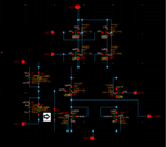
 

Generally as I increase the compensation capacitor the CMFB becomes more stable, because the GBW of the CMFB becomes less and less. This concept is basically should work if I connect it to the output as usual as for any amplifier, again if I would move it to the output it will not work

View attachment 152076

I had similar observations when I designed a fully differential op-amp. The CMFB loop will have as many poles and zeros as the main path as well as some more because of the CMFB amplifier. This makes CMFB amplifier design with HIGH GBW quiet difficult to achieve.

The pitfall of your approach will be that it will be loading your differential amplifier and killing its BW.
 
Dear Vive,

The surprise is that my differential gain characteristics is not at all affected, I am totally happy with the result, only concerned how to scientifically prove that putting capacitor at the input will do the job, how could a reader believe it
 

Without seeing the full CMFB path, it's impossible to decide about the optimal compensation method. The shown capacitor forms a capacitive voltage divider rather than a pole, so I guess it's not optimal. Would be different if you omit the capacitors across the common mode summation network. I would primarily expect some kind of pole splitting respectively miller compensation.
 
Dear Fvm,

Here is the path of my CMFB in the main amplifier, I am taking the average from the output buffer and controlling the down current of the cascode mirror of my folded cascode amplifier,

as you see please, I am controlling half of the down mirror current

Now I think it will be more clear to explain my case

Thank you very much

cct.png
 

Dear FvM

After I replaced the normal resistor with Pseudo MOS resistor, the CMFB loob stability becomes worse even the gain dropped, while the differential gain didn't change,
Also I have noticed that reducing the parallel capacitors to the pseudo resistors will improve the stability,
Below I attached a pic of the Pseudo average resistors

psedue.png
 

I think this way of compensation is good. First, you connected the capacitor from the middle point of the resistor dividers to ground, which means this capacitor is there only for the common mode and is not seen by the differential mode outputs - so, it doesn't affect your differential mode operation, as long as the differential outputs remain well balanced around the common mode voltage.

Second, your averaging resistors and capacitors together with the new capacitor to ground look like a voltage divider for the common mode which has a pole defined by the resistor and the new cap to ground, but it also has a zero because at high frequencies this arrangement reduces to a simple cap divider. Probably, it is that zero that helps with the stability. Or it might be the pole that actually helps because you use pretty high ohmic resistors - 100M, which is an equivalent 50M common mode resistor (it is a separate issue if you can make such a resistor on chip) and the pole it creates with the new cap of 1pF to ground is pushed down to 3.2KHz. You should be able to see which one helps from simulations.

What is the value of the capacitors in parallel with the averaging resistors? It is not well seen from your pictures.
 
Last edited:
Dear Suta,

In my last picture I have replaced the normal resistors with Pseudo MOS resistor, this resistor has very high value in which when I test it in DC it only draw a current in fA.
After connecting it three things happened

1. The CMFB loop gain is dropped largely from 80 dB to 60 dB, differential gain gain or bandwidth still nothing changed
2. I am using 150 fF in parallel with each divider part, the compensation I was added is 1 PF. Now I noticed when I reduce the parallel capacitors from 150 fF to 50 fF the stability becomes better.
3. With the Pseudo transistor resistors, when I disconnect the compensation capacitor the gain is increased.

Hope you can help me in this matter
Thank you all guys
 

I don't quite understand what is happening with those pseudo resistors. Removing the cap shouldn't change your gain for dc or low frequencies. How do you check your gain? Do you just run ac simulation? Did you check you dc operating point with and without the cap? Cap or no cap, the dc op should not change.

Reducing the parallel cap from 150 to 50ff moves the zero by about 3x towards higher frequencies and maybe this movement compensates better a pole and improves stability. Does it happen also when you use regular resistors instead of the pseudo ones?

Frankly speaking, I don't like much these diode connected transistors used as resistors. I were designing the circuit, I'd probably do it differently.
 
Dear Suta, thank you very much for your reply,
indeed capacitors should not change the DC operating point.

I also cant understand how capacitor is changing the DC gain of the CMFB loop, if it is changing the higher frequency gain then I would agree.

I measure the loop gain using the method you always told me by breaking the CMFB loop and inserting iprobe instance and then from STB analyses I see the loop characteristics.

I will answer your other questions when I access the lab and post the simulation result here,

I would like to comment on your last argument, you said you don't like the pseudo connected diode resistors, actually I have simulated it alone and I found that it is working really good as long as the difference voltage at its terminal is kept low, the resistor linearity will be degraded. Therefore I am thinking to stack more diodes in series. Other way I am thinking is to use PMOS pseudo resistor, perhaps I can get more linear range.
Regardless these disadvantages, the implementation of these resistors is very simple and doesnt require a biasing voltage. but if you suggest me other approach, your suggestion is always welcomed

Thank you once again
 

Have you considered using switched-capacitor CMFB? You probably have a clock since you'll be using an ADC after your amplifier.
 
Thank you suta for your reply but my instructor told me that for the moment I have to work with only continuous time circuit
 

Then, is it an option to use source followers connected to the outputs of your amplifier and get the averaging resistors at the output of the source followers? This way you won't lose any differential gain.
 
Thank you suta for your suggestion,

The source follower has two issues, the first it rise considerably the power consumption of the circuit. The second will not work for rail to rail as it is required from my design.
Indeed if you look in to my circuit again, I already have a class AB buffer at the output and it can drive resistive load as well, However the size of my output transistors are right now are (90 um/1 um) for the NMOS, and (240 um/1 um). my circuit performance now is extracted at load = 100 k ohm, CL = 5 PF. If I connect an average resistive load say of 1 kohm this will degrade my performance. In this case I must increase the size of the output transistors which are already big, or you think they are not that big ?

Thank you once again
 

"Big" is a relative thing here.
However, if you say that your output can drive 100K (differential or single ended?) load, then attaching 1M for the averaging resistors is not going to cause much damage since it is 10x larger. But you had in one of your circuits something like 100M which is not practical. No idea what technology you use but many technologies do have reasonable high-ohmic poly resistors.
 
Dear Suta,

The 100 M ohm I had in my design is only for the purpose of simulation, as later I have updated it to the MOS diode pseudo resistors which is not at all consuming area,
 

Did you find out why connecting a capacitor changes you DC loop gain?
 

Actually Suta I didn't go to the lab today.
 

Status
Not open for further replies.

Part and Inventory Search

Welcome to EDABoard.com

Sponsor

Back
Top