Continue to Site

Welcome to EDAboard.com

Welcome to our site! EDAboard.com is an international Electronics Discussion Forum focused on EDA software, circuits, schematics, books, theory, papers, asic, pld, 8051, DSP, Network, RF, Analog Design, PCB, Service Manuals... and a whole lot more! To participate you need to register. Registration is free. Click here to register now.

Miller Op-Amp - PMOS input differential vs NMOS input differential

Status
Not open for further replies.

esdeath_123

Junior Member level 3
Joined
Sep 30, 2018
Messages
25
Helped
0
Reputation
0
Reaction score
0
Trophy points
1
Activity points
235
So, I've encountered two stage miller with PMOS differential pair as input while others have NMOS differential pair input. Are there any advantages/disadvantages of using one over the other? When is it preferable to use a PMOS differential pair as input and when is it preferable to use NMOS differential pair as input?

If you can recommend or know references or materials that discuss this deeply, it would be greatly appreciated. Thanks!
 

The choice is often dictated by the minimum input of the signal. Assume you have a simple OTA with a NMOS input pair, then the minimum input voltage is given by the sum of Vgs across your input pair plus the overdrive of the tail current source. Assume you have an overdrive of 0.2V across the tail current course and an overdrive of 0.2V for the input pair transistors and a Vth of 0.5V. Then the lowest voltage you can apply is 0.9V. On the other hand if your input signal has a large upper voltage, PMOS will be a problem.

The other reasons can be matching. PMOS and NMOS have a different standard deviation of Vth mismatch.

Noise can be different as well which may be another consideration.

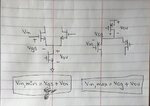
1. To clarify, for large input signal, PMOS will be a problem whereas for small input signal NMOS will be a problem. But why would this be a problem for PMOS or NMOS? Sorry, still kind of confused.
2. Is Vth mismatch a case-to-case basis for NMOS and PMOS? Or like, is one always better than the other?
3. Similar question with previous, regarding noise performance.

If you can recommend references or books with this discussion, it would also be greatly appreciated. I'm still not that knowledgeable with this. Sorry if the questions seem kind of stupid.
 

2019_03_25 8_54 AM Office Lens.jpg
See the attached image as an answer to your first question. Your question was rather unclear. Please be try to be a bit more descriptive. There is no penalty for writing more! :)
Also what do you mean by case to case? PDK to PDK you mean?
 
View attachment 151972
See the attached image as an answer to your first question. Your question was rather unclear. Please be try to be a bit more descriptive. There is no penalty for writing more! :)
Also what do you mean by case to case? PDK to PDK you mean?

Ah, I think I now understand what you mean regarding the input. Sorry if it sounds unclear. I'm just trying to find out when and why a pmos or nmos input can be used. Regarding the case-to-case, what I want to know is, for example, is it always true that using PMOS as input have better standard deviation and noise performance than NMOS as input (or the other way around)? Or will this depend?
 

Regarding to noise, PMOS have smaller flicker noise coefficient, so with same area they produce smaller noise power at lower frequencies than NMOS input stages, always, this is coming from their process.
However the gm of PMOS input stages also smaller (PMOS mobility - µP - always smaller than NMOS's), so over a corner frequency the thermal noise contribution usually bigger for PMOS.
So low bandwidth direct conversion receivers prefer PMOS active mixers for example, but heterodyne or even low-IF mixers have better performance sometimes with NMOS input stages, same true for amplifiers.
Mismatch probably also process dependent, but unfortunately I haven't experienced big differences between the types, I cannot recall a case.
 
Noises and mismatch are process dependent.

In most of the CMOS P-Sub N-Well processes, pfets are placed in n-well, which has to be created in p-sub. It result with one step more with doping the silicon, so it increase variability of doping in pmosfets and thus it worse mismatch coefficient in these processes. It is not true in complementary processes (not used for years N-Sub with P-wells) or in FDSOI, where mismatch for the same transistor flavor is the same. There is an additional story in deca-nanometer CMOS related to halo implantation making mismatch coefficient dimensions and bias dependent.

Flicker noise also depends to the process. Considering CMOS P-Sub N-Well process, pmosfet is created in the n-well, and (omitting physical details) thus it channel is formed deeper than in nmosfet. So, thicker interface layer between channel and oxide results with different mechanism of flicker noise. In such processes, flicker noise in pmosfet is mostly related to fluctuation of carrier mobility and thus is lower and current density dependent (proportional to transconductance - almost constant in weak inversion and prop to square root of current in strong inversion). The channel in nmosfets is formed close to oxide (channel-oxide interface layer is thinner) and flicker noises are generated by interface traps, fluctuating carriers number and thus flicker noises are constant vs operating point and usually much higher. And again, above does not longer true for FDSOI or CMOS with N-Sub and P-Well.

In general, transconductance of both transistor types is the same for the same operating point (with accuracy to slope factor), the difference between p- and n-fets caused by differences in mobility of electrons and holes is in capacitance and thus in transit frequency.

In general, the complementary Miller Op-Amps, designed in the same process, with transistors biased in the same operating point will have almost the same performance - gain, stability, bandwidth, offset, noises and PSRR.
There is a lot of related topics on this forum showing a comparison of complementary opamps also.

Thanks for the reply! If it's not too much trouble, can you provide some links to the topics you mentioned in the forums? I'm not sure if I'm using the correct keywords as I can't seem to find them. Would like to read more about it.
 

View attachment 151972
See the attached image as an answer to your first question. Your question was rather unclear. Please be try to be a bit more descriptive. There is no penalty for writing more! :)
Also what do you mean by case to case? PDK to PDK you mean?

Take a look at chapter 1.1.1 here: https://payhip.com/b/5Srt (CLICK PREVIEW AT THE TOP RIGHT CORNER). Especially, Fig. 1.3 and 1.4. Maybe that could help?
Regarding other resources Razavi and Baker are always good.

Generally, whether it's NMOS or PMOS input stage depends on the specification. If you want to pass 0-1V input signal you choose PMOS input stage. If you have voltage follower for 1V input (e.g voltage reference / bandgap) you may choose NMOS or PMOS. This question is specific. When you have concrete cases it's easier and very often clear. :)

Regarding matching, take a look into foundry documentation. There are plots for matching.
 
Status
Not open for further replies.

Similar threads

Part and Inventory Search

Welcome to EDABoard.com

Sponsor

Back
Top