Continue to Site

Welcome to EDAboard.com

Welcome to our site! EDAboard.com is an international Electronics Discussion Forum focused on EDA software, circuits, schematics, books, theory, papers, asic, pld, 8051, DSP, Network, RF, Analog Design, PCB, Service Manuals... and a whole lot more! To participate you need to register. Registration is free. Click here to register now.

Signal to noise ratio of the operational amplifier

Status
Not open for further replies.

Junus2012

Advanced Member level 5
Joined
Jan 9, 2012
Messages
1,552
Helped
47
Reputation
98
Reaction score
53
Trophy points
1,328
Location
Italy
Activity points
15,235
Dear Friends,

My fully differential amplifier is a part of readout circuit in which I need to drive ADC with 10-12 bit of resolution. This mean that the output of my amplifier must provide signal to noise ratio in this range or resolution.

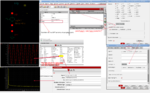
I do a transient simulation and I apply sin signal at the frequency of interest under unity gain connection, then there is a tool by the cadence simulator called "Spectrum" where I can perform the THD from Fourier transform function, it is also giving me the result of the effective number of bits (EFNB), but I am getting like 4 EFNB which is far from of what I expect,

So my questions please are

1. What is the correct simulation setup to find the signal to noise ratio (SNR) at the output of the amplifier ?
2. What is the relationship between the SNR and output referred noise ?

Thank you very much
 
Last edited:

Dear Klaus,

Yes I do it at full scale of output amplitude
 

Tell us how many points you use for the fft, start and stop time for the period you do fft on. You can easily get bad results if you don't set up the simulation correctly.
 
Dear friends,
Thank you very much for your reply,
I will support you with the graph once I reach the lab.

I think you agree that the simulation setup to measure the signal to noise ratio is from the transient analyses with the help of the THD.
Here always a question in my mind, what is the purpose of measuring the output referred noise from the noise analyses, what is the relationship between this noise and the noise from the signal to noise ratio?
 

Hi,

what is the purpose of measuring the output referred noise
It's the only way to get the input referred noise.

N_or = N_ir x (R_f + R_i) / R_i
For both inverting and non-inverting Opamp circuits.
N_ir = input referred noise
N_or = output referred noise
R_i = resistor to inverting input
R_f = feedback resistor

Klaus
 
Dear Klaus, you mean to say there is no relationship between the output noise and the signal to noise ratio, it is only a way to measure input referred noise, (I don't know why cadence give the option of the output noise when it gives the option of the input noise directly)

Dear Suta,
As I promised before, When I go to the lab I will take a picture of the output signal and the spectrum setting so it will be better to discuss,

I would say the you all agree that Spectrum and FFT from cadence is the right simulation to find the SNR, no other way

Thank you very much
 

Dear friends,

I simulated the circuit and brought the results as follow

here is the differential output voltage (Vo1-Vo2) (f=2 MHz, full scale)

1.png

below is the spectrum setting

2.png

and here is the FFT run result

3.png

As you see I am getting 6 bit of resolution, while my intending application is 12 bit !!

I am looking forward for your suggestions and thank you again
 

The effective bits are apparently including THD which isn't noise. The noise floor should be reevaluated with appropriate windowing, it doesn't look trustworthy.

Not sure if the amplifier non-linearity is that high, I would like to see THD versus signal level or IP2 and IP3 figures.
 
Hi,

The FFT result shows that is distortion and not noise that causes bad ENOB.

Try to reduce the signal by 3dB or 6dB to see whether this brings an improvement.


Klaus
 
You are simulating 6 periods of your 2MHz signal. Make sure you select your sampling frequency exactly. The formula for this is Fs(cycles/Npts)=Fx, where Fs - sampling freq, Fx - signal frequency, cycles - number of signal periods, Npts - points in the FFT. Don't start from time 0. Let it simulate for 1 or two periods to let circuit settle any initial transients.
Go to the options of the tran analysis and set the strobeperiod to something like 8 or 16 time smaller than your sampling period and make really sure that your FFT sampling starts on a strobe point which should be guaranteed by linking the strobeperiod to the sampling period. This way you avoid any interpolation that the simulator is doing which also causes non-linearity.
 
Dear Fvm Attached you see below the ''Noise'' simulation which I select from the same spectrum tool, you also please see the result, is that What you wanted to simulate ?

4.png

Dear Klaus, yes exactly when I decrease the amplitude I get higher EFNB (or SNR) from the simulation,

Dear Suta, I am pressing on the S tab which fix automatically the sampling range for the entire signal, I will go next for your suggestion and will provide you with the result ASAP

- - - Updated - - -

only I didn't get how to select the Npts or where to enter it in the simulator
 

Hi,

how does the noise floor look without test signal? (or test signal amplitude very small, like -80dB)

Klaus
 
First off, I think you are only running transient simulation of your amplifier and not transient noise simulation. And you don't have the ADC in the setup. Is that correct? If so, then you don't really have noise from the circuit here. The floor you see is just from the simulator itself.

You are already entering the Npts in your spectrum setup. It is there in the picture you attached.

Say, you want Npts=1024, 6 cycles of the sine wave with a signal frequency of 2MHz. Then your sampling frequency should be 2MHz(1024/6)=341.3333..MHz. Or you can fix the sampling frequency and calculate the exact value of the input frequency. Best is to parametrize it and let spectre calculate it. For example define a variable for Fs, Npts and cycles and create an expression for the input signal sine wave frequency and assign that expression to your input voltage source.


Here, I created a small example of how to set up the dft in cadence and plot the spectrum. It is just for a single sine voltage source but it has all the essentials.

example.PNG
 

Attachments

  • example.PNG
    example.PNG
    492.9 KB · Views: 156
Dear Kluas,
I made the test as you suggested with small input signal (100mVp-p), the result is almost the same as you see below

5.png
6.png

Dear Suta, Yes I didn't do any kind of transient noise or ADC, only I am running the FFT after I run the normal transient simulation , might be the reason ?

for you setting I will try to stay more in the lab to do, but in the pictures you sent me there was no ADC or the Transient Noise, I can see from the ADE one option below the Spectrum called ''Analog to Digital'' is this what you mean by ADC

Thank you friends very much

- - - Updated - - -

****************************************************************************************************************************************************************************************

Dear Suta, I just finished with your setup suggestion, Now I am getting different, Please see the result below

SNRnew.jpg

Just to remind you, I am only using the last setup you told, no ADC no transient noise

Thank you very much in advance
 

"Analog to Digital" in the menue is not what I meant. That option is to convert for example analog waveforms into their digital (0 and 1) representation. For example, if you have a bus with pulses between 0V and 2V, this option can convert it to digital representation in either binary, hex, decimal formats.

When I asked you about the ADC, I really meant analog to digital converter, and you are not using it in your simulations. So, basically you don't have thermal, flicker or quantization noise in your simulation, so you can't really talk about noise there. The noise floor you see in the spectrum comes from the accuracy/rounding errors of the simulator. Unfortunately, it looks like the harmonic distortion is quite real. In your previous plots the 3rd harmonic is at about 40db below fundamental and it is still at 40db below when you used my setup. The only difference is that now, with my setup you force the simulator to be more accurate and its "noise" floor is very much lower compared to your earlier simulations and that's why you can see more harmonics popping up in your spectrum. Before they were below the accuracy noise floor.

You'll have to understand where the nonlinearity of your amplifier comes from. It has a large loop gain, so it must in theory be linearizing the closed loop gain. Look for biasing deficiencies. Maybe you go into slewing, which is basically distortion. Also have a look at the current that goes into your compensation capacitors at the input frequency and amplitude when you do the tran simulation. See if that current is too large so at the peaks of the signal it sucks out big portions of the current from the bias of the stages the compensation cap connects to. This will directly result in non-linearity.
 
Last edited:
Hi,

I made the test as you suggested with small input signal (100mVp-p),
If 100mV is about -80dB ....
Then the FS signal amplitude is about 1000V. ;-)

It rather looks like you reduced the amplitude by 25dB only..

*****
The new diagram shows that the whole problem is not related to noise, but it's a problem of the measurement setup.
Or better say: the frequencies...

Try to rectify the frequencies...
Or use a windowing function as workaround.

Klaus
 
"Analog to Digital" in the menue is not what I meant. That option is to convert for example analog waveforms into their digital (0 and 1) representation. For example, if you have a bus with pulses between 0V and 2V, this option can convert it to digital representation in either binary, hex, decimal formats.

When I asked you about the ADC, I really meant analog to digital converter, and you are not using it in your simulations. So, basically you don't have thermal, flicker or quantization noise in your simulation, so you can't really talk about noise there. The noise floor you see in the spectrum comes from the accuracy/rounding errors of the simulator. Unfortunately, it looks like the harmonic distortion is quite real. In your previous plots the 3rd harmonic is at about 40db below fundamental and it is still at 40db below when you used my setup. The only difference is that now, with my setup you force the simulator to be more accurate and its "noise" floor is very much lower compared to your earlier simulations and that's why you can see more harmonics popping up in your spectrum. Before they were below the accuracy noise floor.
.

Dear Suta, I dont know how to thank you really for your kind help, every point you say is really useful

Now I would like to reply to your points, As I can understand from you that because I don't have an ADC or such sampling circuit with my chip it means there is no need to measure the Signal to Noise Ratio , However I saw some papers where people giving the SNR of their op-amp, also they provide dynamic range in dB which I think it is the same the SNR.

Suppose I have sampling or any source of thermal or flicker, is it still the same setup to do to find the SNR ? from my obtained signal how much is SNR ? do I need to send the signal to different function in calculator to do it

Dear Suta, so you mean that spectrum and your setting is the same function but more details or accuracy is given by your method.

Regarding the THD, yes I have 1.3 % THD. The GBW of my amplifier is 16 MHz and the Slew rate is 40 V/u.s, the applied test signal is 0.9 Vp-p... I would say surely when we reduce the amplitude we reduce the harmonic distortion, when we avoid slewing the signal we improve the linearity, the last source left for the non linearity is the loop gain which decrease with frequency, do you think GBW = 16 MHz can not cover 2 MHz signal ??, However I have tested the closed loop gain at this frequency, it is giving me 0.988 rather than unity as I configured it as a buffer.

I have couple of questions about your setup, but I would post it later please

- - - Updated - - -

Hi,


If 100mV is about -80dB ....
Then the FS signal amplitude is about 1000V. ;-)

It rather looks like you reduced the amplitude by 25dB only..

*****
The new diagram shows that the whole problem is not related to noise, but it's a problem of the measurement setup.
Or better say: the frequencies...

Try to rectify the frequencies...
Or use a windowing function as workaround.

Klaus

Dear Klaus,

Thank you very much for your help,

There is option of the used window in the spectrum, is that what you meant to change ?

- - - Updated - - -

The effective bits are apparently including THD which isn't noise. The noise floor should be reevaluated with appropriate windowing, it doesn't look trustworthy.

Not sure if the amplifier non-linearity is that high, I would like to see THD versus signal level or IP2 and IP3 figures.

Dear FvM,
Thank you a lot

The same question :) what is the appropriate windowing?

if you look to the time domain of my signal you can say it has very low non linearity but after applying FFT I am getting 1.2 %,

Sorry I didn't understand of IP2 and IP3
 

I assume that the "noise floor" in some measurements is caused by a rectangular FFT window not corresponding exactly to an integer number of sine periods. You'll better use something like a Hann window.

As already stated by others, there are no noise sources modelled in a transient simulation, thus you'd expect a much lower spurious signal floor due to numerical inaccuracy. THD in contrast seems to be real, the non-linearity is designed into your amplifier. GBW of 16 MHz is not sufficient to reduce it by means of feedback for a 2 MHz signal.
 
Status
Not open for further replies.

Part and Inventory Search

Welcome to EDABoard.com

Sponsor

Back
Top