Continue to Site

Welcome to EDAboard.com

Welcome to our site! EDAboard.com is an international Electronics Discussion Forum focused on EDA software, circuits, schematics, books, theory, papers, asic, pld, 8051, DSP, Network, RF, Analog Design, PCB, Service Manuals... and a whole lot more! To participate you need to register. Registration is free. Click here to register now.

VFD to control 3 phase AC induction motor 400V 6000 rpm

Status
Not open for further replies.
Hi,

Use a scope to check the signals into the gate driver.

Klaus
 

Did you ever check the waveforms generated by your control circuit in a simulation or measurement? As previously mentioned, the circuit looks completely wrong to me. I fear a basic misunderstanding of required inverter switching pattern.

I would expect each half bridge switching according a sine pwm waveform as shown below (pwm frequency not to scale). High and low side switch are actived alternatingly with some deadtime.

sinepwm.PNG

To achieve maximum output voltage with 3x120° output, a "zero sequence" signal need to be superimposed, see the discussion in a previous thread.
https://www.edaboard.com/showthread...-3-phase-VFD&p=1617141&viewfull=1#post1617141

The control signals can be generated purely digitally by a slightly more powerful processor, e.g. dsPIC or ARM with respective PWM block.
 

Is your power supply 560VDC? (That is the peak for a nominal 400VAC waveform.) What voltage does your control circuit apply to the gates?

Perhaps you have Pmos/PNP in your half-bridge? Then to turn off a Pmos/PNP you must apply the same volt level at its gate, as the voltage at its more positive terminal.

To turn it on you might not be safe to pull the gate to 0V. The insulated gate might not tolerate such large voltage differential.

The H-bridge circuit in my simulation (post #8) is formed by two op amps. I used them as 'cheats' to make it easy for me. However it's a good idea to make a simulation with 6 op amps connected to apply waveforms to a 3-phase motor. I suppose the half-bridges contact each other, so there's a chance one of them creates a short circuit with another at overlapping times in the cycle.
 

Hi,

Use a scope to check the signals into the gate driver.

Klaus

Did you ever check the waveforms generated by your control circuit in a simulation or measurement? As previously mentioned, the circuit looks completely wrong to me. I fear a basic misunderstanding of required inverter switching pattern.

I would expect each half bridge switching according a sine pwm waveform as shown below (pwm frequency not to scale). High and low side switch are actived alternatingly with some deadtime.

View attachment 151955

To achieve maximum output voltage with 3x120° output, a "zero sequence" signal need to be superimposed, see the discussion in a previous thread.
https://www.edaboard.com/showthread...-3-phase-VFD&p=1617141&viewfull=1#post1617141

The control signals can be generated purely digitally by a slightly more powerful processor, e.g. dsPIC or ARM with respective PWM block.

Is your power supply 560VDC? (That is the peak for a nominal 400VAC waveform.) What voltage does your control circuit apply to the gates?

Perhaps you have Pmos/PNP in your half-bridge? Then to turn off a Pmos/PNP you must apply the same volt level at its gate, as the voltage at its more positive terminal.

To turn it on you might not be safe to pull the gate to 0V. The insulated gate might not tolerate such large voltage differential.

The H-bridge circuit in my simulation (post #8) is formed by two op amps. I used them as 'cheats' to make it easy for me. However it's a good idea to make a simulation with 6 op amps connected to apply waveforms to a 3-phase motor. I suppose the half-bridges contact each other, so there's a chance one of them creates a short circuit with another at overlapping times in the cycle.

My IGBT bridge is connected to my lab PSU at 30V 1A right now
The gate voltage is 15V
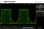
I check the signals into the LM358 comparators - positive inputs and coresponding output.
CH1 POSITIVE INPUT -> CH2 OUTPUT

20190324_225930.jpg

The output waveform is correct ?

Thank you
 
Last edited:

Hi,

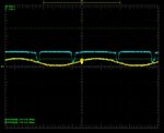
I check the signals into the LM358 comparators - positive inputs and coresponding output.
CH1 POSITIVE INPUT -> CH2 OUTPUT
...

The output waveform is correct ?

A comparator's output should be digital, either HIGH or LOW.
I don't even know which color is which signal.
The one is not digital, the other doesn't go LOW...
The one frequency is twice the frequency of the other...
And both are noisy..

I'm really curious about the solution to your riddle.

Klaus
 

hi,


a comparator's output should be digital, either high or low.
I don't even know which color is which signal.
The one is not digital, the other doesn't go low...
The one frequency is twice the frequency of the other...
And both are noisy..

I'm really curious about the solution to your riddle.

Klaus

ch1 positive input (yelow) -》ch2 output (blue)
 

I can't relate the output waveform to the previously posted "control circuit". It looks like a window comparator output signal, which suggests that the real circuit is different from the posted schematic.
 

Hi,

If we buy everything as we develop ourselves? How about the passion for electronics? I think it's far more beneficial if I solve this problem here - I think many of our children will have a lot to learn. So the benefit would be millions of times bigger than if I bought a VFD.
I don´t agree.
You try to re-invent the wheel .. but without knowing about the opreration principle.
Many others have done motor control before. Thus there is a lot of documentiation how this works.

* Please first learn the theory,
* then draw some overview, show signal flow charts and timing diagrams of what you expect (hand drawn is fine).
(I can´t see what how your circuit should work. Neither from the schematic, nor from your description)
* Then start to build the hardware.
* then verify the signals - step by step - with your expected values.

That´s the way we professionals need to go - to get good results. So why not you, too?

****
Just explain:
To me it seems you generate PWM with using DDS. Then you generate analog signals. Then you generate PWM signals again...
Thus: Digital --> analog --> digital.
Why not directly use the DDS PWM? (Without analog)

****
Your signals (scope) seem to be very noisy and don´t have the correct voltage levels.
It looks like you try to use a breadboard to desgin a switched power application.
If so, you should have learned from other threads here, that this often is just a waste of time.
--> a breadboard is not suitable for this application.

Kaus
 

I can't relate the output waveform to the previously posted "control circuit". It looks like a window comparator output signal, which suggests that the real circuit is different from the posted schematic.

Hi,


I don´t agree.
You try to re-invent the wheel .. but without knowing about the opreration principle.
Many others have done motor control before. Thus there is a lot of documentiation how this works.

* Please first learn the theory,
* then draw some overview, show signal flow charts and timing diagrams of what you expect (hand drawn is fine).
(I can´t see what how your circuit should work. Neither from the schematic, nor from your description)
* Then start to build the hardware.
* then verify the signals - step by step - with your expected values.

That´s the way we professionals need to go - to get good results. So why not you, too?

****
Just explain:
To me it seems you generate PWM with using DDS. Then you generate analog signals. Then you generate PWM signals again...
Thus: Digital --> analog --> digital.
Why not directly use the DDS PWM? (Without analog)

****
Your signals (scope) seem to be very noisy and don´t have the correct voltage levels.
It looks like you try to use a breadboard to desgin a switched power application.
If so, you should have learned from other threads here, that this often is just a waste of time.
--> a breadboard is not suitable for this application.

Kaus

Hello,
I followed this project with small changes: https://www.dropbox.com/s/cyy5bru3nvh90n5/Design%20Strategy%20for%20a%20%203-Phase%20Variable%20Frequency%20Drive%20%28VFD%29.pdf?dl=0

For example I changed LM339 with LM358 and 4011NAND with 74HC00N
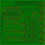
This is my control board pcb ctrlbrd.jpg
This is my test pcbs: work.jpeg , pcb1.jpeg , gatedriver.jpeg
I think my oscilloscope is the blame for those noises - I have a Hantek and I think it is of poor quality.
I hope to get a better performance oscilloscope to make higher accuracy measurements.
Until then, please analyze these circuits and tell me what's wrong here.
Thank you
 
Last edited:

Hi,

For example I changed LM339 with LM358
One is a comparator, the other is an OPAMP. The both (sadly) use the same schematic symbol,
* but the OPAMP is designed for low differential input voltages and analog output
* but the COMPARATOR is designed for high differential input voltages and digital output

There are many other differences.

When you replace parts, then you should know why and how to replace them. The ouput signal will differ a lot. In timing in function and in signal levels. .... this is what I mean with "learning the theory first"

***
Your PCB is single layer without GND plane. Expect EMI/EMC problems and increased noise. A copper pour is no solid, low impedance GND plane.
The reference design uses 2 layers with GND plane. --> If you modify this, you should know why and how and waht are the risks.

***
The wiring is a mess. This is not how a "switching power" application needs to be wired. You need to take care about wire lengths, ground bounce, return paths.
Ground bounce is caused by high currents, high dI/dt, signal loop impedance...

***
Scope:
This is the smallest problem.

***
My recommendation: Read application notes from reliable sources. Many semiconductor manufacturers (IGBT, MOSFET, gate driver IC...) provide such documents.
They are for free, so use them. They provide this documents because they see the need for it. Even experienced electronics designers should read them when they enter the new filed of "power electronics". There´s a good reason for it.

*****
I see a lot of mistakes. No wonder the result is not what you expect.

Believe me, I would be gald if I coud tell you: "modify the value of resistor X and everything will work". But this isn´t the case.
Designing a 6kW VFD isn´t simple. It is complex. It is complex from the theory and from the hardware design. There are so much pitfalls...

Klaus
 
Hi,


One is a comparator, the other is an OPAMP. The both (sadly) use the same schematic symbol,
* but the OPAMP is designed for low differential input voltages and analog output
* but the COMPARATOR is designed for high differential input voltages and digital output

There are many other differences.

When you replace parts, then you should know why and how to replace them. The ouput signal will differ a lot. In timing in function and in signal levels. .... this is what I mean with "learning the theory first"

***
Your PCB is single layer without GND plane. Expect EMI/EMC problems and increased noise. A copper pour is no solid, low impedance GND plane.
The reference design uses 2 layers with GND plane. --> If you modify this, you should know why and how and waht are the risks.

***
The wiring is a mess. This is not how a "switching power" application needs to be wired. You need to take care about wire lengths, ground bounce, return paths.
Ground bounce is caused by high currents, high dI/dt, signal loop impedance...

***
Scope:
This is the smallest problem.

***
My recommendation: Read application notes from reliable sources. Many semiconductor manufacturers (IGBT, MOSFET, gate driver IC...) provide such documents.
They are for free, so use them. They provide this documents because they see the need for it. Even experienced electronics designers should read them when they enter the new filed of "power electronics". There´s a good reason for it.

*****
I see a lot of mistakes. No wonder the result is not what you expect.

Believe me, I would be gald if I coud tell you: "modify the value of resistor X and everything will work". But this isn´t the case.
Designing a 6kW VFD isn´t simple. It is complex. It is complex from the theory and from the hardware design. There are so much pitfalls...

Klaus

My pcb is single layer but have ground plane WhatsApp Image 2019-03-16 at 13.48.03.jpeg

"" One is a comparator, the other is an OPAMP. The both (sadly) use the same schematic symbol,
* but the OPAMP is designed for low differential input voltages and analog output
* but the COMPARATOR is designed for high differential input voltages and digital output ""
This is information that helps me a lot.
That's why we have called on you professionals.
Thank you for that
 

Thanks for sending the project report. Unfortunately I'm still unable to understand the exact idea behind the control circuit. It may work somehow, but is far from a reasonable VFD design. Particularly it's unable to drive the reactive motor load appropriately. I wonder if the author has ever run it with a real motor.

An important difference between your and the original design is that the original design uses a driver that locks high and low side with deadtime. If the control logic generates overlapping gate signals (it actually does at first look), it does no harm there.
 

Hi,

My pcb is single layer but have ground plane
No. You have copper pour - this is far away from the GND plane of the reference design.

Mind:
You are not designing a DC application. A trace is not only DC resistance anymore it becomes a complex imedance.

You are not the first one trying to design a VFD (or any other swithicng power application) and you are not the first one making mistakes. Thus there arey many threads discussing the same.

A forum is meant that you gain from former discussions. Don´t be surprised if the ones who want to help don´t repeat the same again and again but refer to existing threads. (and school and application notes and reliable reference designs and ...)

Klaus

I wonder if the author has ever run it with a real motor.
Me too.
 
Hi,


No. You have copper pour - this is far away from the GND plane of the reference design.

Mind:
You are not designing a DC application. A trace is not only DC resistance anymore it becomes a complex imedance.

You are not the first one trying to design a VFD (or any other swithicng power application) and you are not the first one making mistakes. Thus there arey many threads discussing the same.

A forum is meant that you gain from former discussions. Don´t be surprised if the ones who want to help don´t repeat the same again and again but refer to existing threads. (and school and application notes and reliable reference designs and ...)

Klaus


Me too.

Another useful information - I'm here to learn "No. You have copper pour - this is far away from the GND plane of the reference design."
https://www.edaboard.com/showthread.php?25701-Any-different-btw-copper-pour-amp-ground-plane
And now something very interesting but not upset about me about the wires and the ground plan....
Do you say that this man has a ground plan and his wires are more orderly than mine? :))) https://www.youtube.com/watch?v=INI3OD7YE9g&feature=youtu.be
However his motor is spinning ...
Thank you
 
Last edited:

Hi,

Do you say that this man has a ground plan and his wires are more orderly than mine? :)))
It´s not about "orderly", it´s about impedance.

How many fake videos are out there? I don´t know if this is one.

But ask yourself: Why does he move the pot to run the motor instead of running it via the microcontroller?

And as said before... and underlined before.

Maybe this video is no fake and the motor is spinning because everything is working..
What do you think will happen when one moves one wire 5cm away from it´s current position?
How long did he test and fail until it is running "by accident"?

I´ve underlined the word "reliable".
Because there are so many circuits around the work now, but not the next time. They work now but nit at different temperature. They work now, but you can´t hear radio anymore because the circuit causes too much EMI. They work now, but refuse to work when there is WiFI, Bluetooth, cellular phone... nearby, because they catch u any EMI noise.

I´ve seen so many bad designs causing trouble ... and angry customers...

***
And to be honest. After many years of school I had not all the knowledge to buid a 6kW drive. One needs to go step by step. For years.
And one needs experience (and fails), best from small power DC drives to higher power DC drives to AC drives.

At leat this is true for me. But I´m not perfect, but after decades of desiging electronics I have a good chance to get it running - reliably.

And still I need to read lots of datasheets, application notes... every day! Technology doesn´t stop. New semiconductros, new applications, new requirements, new regulations ...

I do many designs for high power industry.
There are systems running from the 1970s. But now causing problems. Not because they are old.
In the 1970s there were no cellular phones and no WiFi... thus the EMC requirement has changed...

Klaus
 

Thanks for sending the project report. Unfortunately I'm still unable to understand the exact idea behind the control circuit. It may work somehow, but is far from a reasonable VFD design. Particularly it's unable to drive the reactive motor load appropriately. I wonder if the author has ever run it with a real motor.

An important difference between your and the original design is that the original design uses a driver that locks high and low side with deadtime. If the control logic generates overlapping gate signals (it actually does at first look), it does no harm there.

Hi,


No. You have copper pour - this is far away from the GND plane of the reference design.

Mind:
You are not designing a DC application. A trace is not only DC resistance anymore it becomes a complex imedance.

You are not the first one trying to design a VFD (or any other swithicng power application) and you are not the first one making mistakes. Thus there arey many threads discussing the same.

A forum is meant that you gain from former discussions. Don´t be surprised if the ones who want to help don´t repeat the same again and again but refer to existing threads. (and school and application notes and reliable reference designs and ...)

Klaus


Me too.

Hi,


It´s not about "orderly", it´s about impedance.

How many fake videos are out there? I don´t know if this is one.

But ask yourself: Why does he move the pot to run the motor instead of running it via the microcontroller?

And as said before... and underlined before.

Maybe this video is no fake and the motor is spinning because everything is working..
What do you think will happen when one moves one wire 5cm away from it´s current position?
How long did he test and fail until it is running "by accident"?

I´ve underlined the word "reliable".
Because there are so many circuits around the work now, but not the next time. They work now but nit at different temperature. They work now, but you can´t hear radio anymore because the circuit causes too much EMI. They work now, but refuse to work when there is WiFI, Bluetooth, cellular phone... nearby, because they catch u any EMI noise.

I´ve seen so many bad designs causing trouble ... and angry customers...

***
And to be honest. After many years of school I had not all the knowledge to buid a 6kW drive. One needs to go step by step. For years.
And one needs experience (and fails), best from small power DC drives to higher power DC drives to AC drives.

At leat this is true for me. But I´m not perfect, but after decades of desiging electronics I have a good chance to get it running - reliably.

And still I need to read lots of datasheets, application notes... every day! Technology doesn´t stop. New semiconductros, new applications, new requirements, new regulations ...

I do many designs for high power industry.
There are systems running from the 1970s. But now causing problems. Not because they are old.
In the 1970s there were no cellular phones and no WiFi... thus the EMC requirement has changed...

Klaus
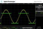
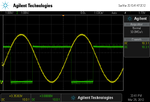
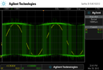
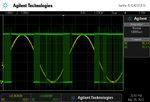
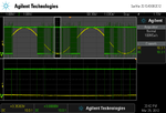
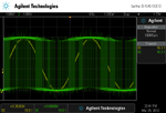
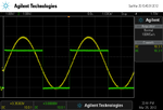
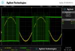
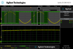
I measured again with another scope.
Yelow signal are the reference sinusoidal signal:
OpAmp-Pin7 H out 03 OpAmp-Pin7 H out.png
OpAmp-Pin1 L out 06 OpAmp-Pin1 L out.png

07 NAND-Pin2 IN1a.png
08 NAND-Pin1 IN1b.png
09 NAND-Pin3 OUT1.png
10 NAND-Pin3 OUT1 NOT OK FOR ME.png
NAND-Pin6 OUT AHigh 11 NAND-Pin6 OUT2.png
12 NAND-Pin12 IN3a.png
13 NAND-Pin11 OUT3.png
14 NAND-Pin11 OUT3 OK.png
NAND-Pin8 OUT ALow 15 NAND-Pin8 OUT4.png

I named all pictures with the coresponding measurement.
What is not good here ?
 
Last edited:

Hi,

very doubtful.

I wonder how the sine amplitude can be 0V/5V with your given circuit.
It´s simply impossible ... at least in my eyes.

Klaus
 

Hi,

very doubtful.

I wonder how the sine amplitude can be 0V/5V with your given circuit.
It´s simply impossible ... at least in my eyes.

Klaus

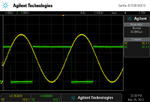
I disconnected R2 270 ohm resistor now and i adjust the sinusoidal signal with the R3 100K POT
Screenshot 2019-03-25 17.00.22.png
 

Hi,

what else should we know???
How many modifications did you make! ... and you want us to rectify it ...

Klaus
 

Status
Not open for further replies.

Similar threads

Part and Inventory Search

Welcome to EDABoard.com

Sponsor

Back
Top