Continue to Site

Welcome to EDAboard.com

Welcome to our site! EDAboard.com is an international Electronics Discussion Forum focused on EDA software, circuits, schematics, books, theory, papers, asic, pld, 8051, DSP, Network, RF, Analog Design, PCB, Service Manuals... and a whole lot more! To participate you need to register. Registration is free. Click here to register now.

Effect of Gds on Gain

Status
Not open for further replies.

shruthi08

Newbie level 5
Joined
Oct 2, 2018
Messages
8
Helped
0
Reputation
0
Reaction score
0
Trophy points
1
Activity points
69
Hello

I am designing a differential active balun at 28GHz frequency with pmos as load instead of resistors to increase the gain. After DC simulations I have gds = 17.83mS and a gain of 0dB.
The circuit has been matched at the input and output.

Are there methods to decrease the value of gds?

Vdd = 1V
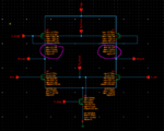
Schematic_DiffAB.PNG
 

I see your drain current is 3.7 mA. you must have a very large width to source that much current. You'll have a larger output resistance (1/gds) at microlevel current.
 

Increase the load device lengths.
 

Yes, the PMOS transistors are near triode region. The gm of the PMOS is almost the same as gds. Youu can't expect to get reasonable gain like this.
 

Thank you everyone for pointing out where im going wrong. I will check the bias voltages again and make sure the transistors are well in saturation.
 

Missing from the discussion thus far is the load / termination,
absent from the subcircuit view shown. At such frequencies
I'd expect this to be a design challenge and to dominate
node impedances - perhaps to the point that your PMOS
load ought to instead be a well behaved RF resistor, capacitor
blocked from the next stage's input?

17mS just happens to be pretty close to 50 ohms. Though
this is a bit low for low power RF receiver chains on-chip,
it might be proper to have the whole 28GHz lineup put to
50 ohms and forget active loads?
 

Thank you guys,

I have done input and output impedance matching in the test bench(below). I followed the suggestions given above and realised a gain of 7dB.

DAB_tb_1.PNG

- - - Updated - - -

I found another discrepency wrt to the gain analysis for S21 and S31. My RFout1 and RFout2 ports should be equal in magnitude but out of phase by 180degrees. With transient analysis I see a difference in amplitude for the output signals.

The schematic is symmetric wrt the drain of current source transistor. Is there a reason I am missing for this discrepency?

DAB_gain_ideal.PNG DAB_trans.PNG
 

Small signal they might look equal but large signal,
you are pulling the tail and compressing Vds cyclically
so your gain and common mode position are varying.
This leads to distortion and harmonic generation.

Schematic symmetry does not imply operating point
symmetry at large signal across the cycle.
 

0 --> cut-off
1 --> triode
2 --> saturation
3 --> subthreshold
4 --> breakdown (I am not sure about this)

- - - Updated - - -

Thank you guys,

I have done input and output impedance matching in the test bench(below). I followed the suggestions given above and realised a gain of 7dB.

View attachment 151901

- - - Updated - - -

I found another discrepency wrt to the gain analysis for S21 and S31. My RFout1 and RFout2 ports should be equal in magnitude but out of phase by 180degrees. With transient analysis I see a difference in amplitude for the output signals.

The schematic is symmetric wrt the drain of current source transistor. Is there a reason I am missing for this discrepency?

View attachment 151902 View attachment 151903

You need to do a PSS simulation for analyzing these type of blocks. A transient is not the correct picture.
 

If the Gds=17mS leads to the drain impedance of the PMOS to be 50 ohm, whether the PMOS can not go to the saturation region? Gds with 17mS is too high for the transistor in the saturation region. Is it correct?
 

Depends on your criteria for high as well as the size of the transistor and the current through it.
 
Status
Not open for further replies.

Part and Inventory Search

Welcome to EDABoard.com

Sponsor

Back
Top