Continue to Site

Welcome to EDAboard.com

Welcome to our site! EDAboard.com is an international Electronics Discussion Forum focused on EDA software, circuits, schematics, books, theory, papers, asic, pld, 8051, DSP, Network, RF, Analog Design, PCB, Service Manuals... and a whole lot more! To participate you need to register. Registration is free. Click here to register now.

How to design an class d output filter ( active filter )?

Status
Not open for further replies.

c75739

Newbie level 2
Joined
Mar 17, 2019
Messages
2
Helped
0
Reputation
0
Reaction score
0
Trophy points
1
Activity points
32
I want to filter output of my full-bridge class d power amp. I'm trying to connect an ideal differential op to class d output for simulation. But class d output through ideal differential op , growing noise floor(5~10dB). I suspect that problem is incorrect op/filter connection. (pic. A)
123.png
pic.A

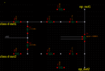
First, I'm mapping circuit(pic. A) to spectre(use one VCVS(pic. B) or two VCVS(pic. C)). I'm trying 2 connections below:

001.png
pic. B one VCVS class d output SNDR is 96dB, op(ideal, gain: 100000) out is 82 dB problem is that op is ideal, 96dB to 82dB doesn't make sense.

002.png
pic. C two VCVS class d output SNDR is 96dB, op(ideal, gain: 100000) out is 74 dB problem is that op is ideal, 96dB to 74dB doesn't make sense.

I think SNDR of ideal differential op output, sholdn't decrease much.

Does the connection of op(pic.B or pic.C) is correct? Any suggestion?
Thankyou!!!!
 

Seriously I don't understand the purpose of an active filter behind a class D amplifier. Nevertheless a linear filter with almost flat pass band (it's actually a 1.5 dB ripple Chebyshev) can hardly worsen SNDR, thus I presume you are calculating it somehow incorrect.

- - - Updated - - -

Does the connection of op(pic.B or pic.C) is correct?
None of it could be implemented as a real circuit, but both should work with ideal sources. A real fully differential amplifier need a CMFB stage.
 

Hi,

Just use a passive filter. It should be calculated according real used load impedance.

Klaus
 

When I hear class-D I assume its a switching power amplifier chosen for high efficiency. Adding a linear active filter afterward throws the efficiency, and the reason for the class-D, out the window.

I hope these are simply pulse with modulated I/Os, in which case this has a chance of making some sense.
 

Hi,

Adding a linear active filter afterward throws the efficiency, and the reason for the class-D, out the window.
1) choosing the right devices may not significantely drop the efficiency
2) compared with the OP's solution to use an active filter --> the efficiency of the class D amplifier becomes meaningless at all

Klaus
 

I think we agree, I was sloppy with terminology perhaps.
 

thanks for your suggestion!

My DAC chip is included delta-sigma modulator and class D amplifier.
The active filter is connected off chip, so I use an ideal differential op in Spectre to model a filter off chip.
I think an active filter behind a class D amplifier can reduce the size of my class D amplify MOSFET and be low power of my chip.

Voltage of my class D output is 3 level(1.8V, 0.9V, 0V), so I give 0.9V to the filter for common mode voltage. like pic. A.
Is it correct?

I agree with you entirely that a linear filter can hardly worsen SNDR. I will check again my calculate code.
I really appreciate your help.
 

Purpose of the design is still mysterious. You may use a SD-modulator to drive a three-level class D amplifier and place a passive LC filter towards the load to remove switching frequency. You also may connect an active filter to the class D amplifier output to monitor the output signal, although you can better tap the voltage after the passive LC filter.

I think an active filter behind a class D amplifier can reduce the size of my class D amplify MOSFET.
Not if the class D is intended to source power to a load. If not, why are you using class D?
 

Status
Not open for further replies.

Similar threads

Part and Inventory Search

Welcome to EDABoard.com

Sponsor

Back
Top