Continue to Site

Welcome to EDAboard.com

Welcome to our site! EDAboard.com is an international Electronics Discussion Forum focused on EDA software, circuits, schematics, books, theory, papers, asic, pld, 8051, DSP, Network, RF, Analog Design, PCB, Service Manuals... and a whole lot more! To participate you need to register. Registration is free. Click here to register now.

[ADS] Design of spiral inductor In ADS

Status
Not open for further replies.

pragash

Advanced Member level 2
Joined
Jul 4, 2005
Messages
512
Helped
64
Reputation
128
Reaction score
59
Trophy points
1,308
Location
Oakland
Activity points
4,940
im designing spiral inductor in ADS using passive circuit design guide. my question is what H (substrate thickness) should i set in the MSUB? Spiral should not have any ground plane underneath. due to this, shall i set the H to be the total H of the PCB since im placing the spiral on the top layer?

if im placing the spiral on the 2nd layer, shall i use the same MSUB and set the H to be the total H of the PCB minus the H of the top layer?
 

my question is what H (substrate thickness) should i set in the MSUB? Spiral should not have any ground plane underneath. due to this, shall i set the H to be the total H of the PCB since im placing the spiral on the top layer?

It's good to have no ground below, but I wonder how accurate the model is in that case. I would set a very large height for the model's MSUB, to minimize the (missing) eddy current effect of the (missing) ground underneath.

The major effect that we expect from such an inductor is series R+L, with some parasitic C between the inductor turns. By making the MSUB's H large, you decrease the shunt capacitance to ground (correct because no ground below) and the impact of ground on series L (correct because no ground below).

With no ground below, the difference between your two inductor placements (top and middle layer) is only the effect of FR4 on parasitic capacitance betweem the turns. Or in other words: self resonance frequency. But I suspect that the "abused" microstrip inductor model isn't very accurate anyway, so I wouldn't worry about that second order effect.

~~

Looking at your previous layouts, I think you will have a large effect (inductancce error) from metal on other layers that creates a closed loop around your inductor. That isn't included in your microstrip inductor model, so you need to check that using EM anyway.
 
With no ground below, the difference between your two inductor placements (top and middle layer) is only the effect of FR4 on parasitic capacitance betweem the turns. Or in other words: self resonance frequency. But I suspect that the "abused" microstrip inductor model isn't very accurate anyway, so I wouldn't worry about that second order effect.

~~
Dr Volker, thanks for your comments. just one input. L value on 2nd value will be higher than the 1st layer due to T difference. 1st layer is 0.7mil whereas 2nd layer is 1.4mils. thank you very much.

- - - Updated - - -

It's good to have no ground below, but I wonder how accurate the model is in that case. I would set a very large height for the model's MSUB, to minimize the (missing) eddy current effect of the (missing) ground underneath.

since we are removing all the layers underneath, I believe the H has to be the total H of the PCB. Only then the actual scenario will be portrayed in the simulation. I don't understand why you worried about the accuracy. Please explain further on this point.

- - - Updated - - -

Looking at your previous layouts, I think you will have a large effect (inductancce error) from metal on other layers that creates a closed loop around your inductor. That isn't included in your microstrip inductor model, so you need to check that using EM anyway.

currently im locating the spiral in the 2nd layer, just below the top layer. this is to avoid adjacent interferer and also increase the inductance because 2nd layer T is double the T of top layer. this is for space saving. since the spiral is in 2nd layer, i can just create keep out the size of the inductor at all other layers.
 

just one input. L value on 2nd value will be higher than the 1st layer due to T difference. 1st layer is 0.7mil whereas 2nd layer is 1.4mils.

Sure, then use separate MSUB for each inductor.

since we are removing all the layers underneath, I believe the H has to be the total H of the PCB.

No, you should set H to a very large value. If you set H to the substrate height, you will get results for an inductor over solid ground plane. Inductor over solid ground plane has much different (poor) performance, because the ground totally changes the magentic field distribution. We discussed that in your earlier threads on the same topic.

I don't understand why you worried about the accuracy.

For best inductor performance we want to remove the ground. The microstrip inductor model is designed for microstrip inductor. That's the difficulty. I have doubts how accurate the model is when removing the ground, because it was not designed to for that case. My proposal is to set H to a large value (ground far away), but I never tried how good results are then.

and also increase the inductance because 2nd layer T is double the T of top layer.

I'm a bit surprised that you see much effect of the trace width. For spiral inductors, that is usually a small effect.

~~~

I this was my project: forget schematic models and only trust EM (Momentum).
 
For best inductor performance we want to remove the ground. The microstrip inductor model is designed for microstrip inductor. That's the difficulty. I have doubts how accurate the model is when removing the ground, because it was not designed to for that case. My proposal is to set H to a large value (ground far away), but I never tried how good results are then.

ok got it. thanks.

- - - Updated - - -

Dear dr. Volker,
im setting the H to be 1000000000 mil. i will share the correlation between schematic simulation and layout simulation for your information.
 

Dr Volker,
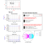
i have some confusion here which needs clarification. i designed 1nH spiral using passive design guide. LnH shows clean response without any resonance. please see the pictures below.
passive.png
passive DG2.png
passive DG1.png

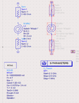
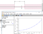
i simulated the same spiral in ADS circuit with the same stack up. the response looks different at the circuit simulation with resonance (SRF) within the frequency of interest. im confused on why is it happening. is it because passive design guide is inaccurate? im using ADS 2-port spiral inductor template for this simulation. please see pictures below.

circuit simulation with 2-port spiral DDS_2.png
circuit simulation with 2-port spiral DDS.png
circuit simulation with 2-port spiral DDS_1.png

- - - Updated - - -

i dont know why passive design guide doesnt correlate with spiral circuit simulation in terms of Leff. Please advice.
 

LnH shows clean response without any resonance. please see the pictures below.

I never used that design guide. The curve looks very ideal, I wonder if the design guide uses a very simple equation. Or maybe it is correct and 0.5 turn -> 1nH is really so flat at these frequencies.

In your schematic, you have "radius = 20" with no units. That might result in 20 meter (not 20 mils).

~~~

I understand that your spirals have no ground below. For spiral inductors with no ground below, can you use these equations to estimate the low frequency (DC) inductance:
https://www.circuits.dk/calculator_planar_coil_inductor.htm

Then, use Momentum simulation to get the wideband results (frequency response).

~~~

For the curves in your data display, autoscaling didn't work well. You need to set the y axis manually, otherwise it's difficult to see the response.
 
Last edited:
Ri=20mils ( 0.508mm)
S=3mils ( 76.2um )
W=3mils ( 76.2um)

These values are absurd.
In order to get a realistic values from ANY model of a component ( active or passive ) the dimensions ( or other parameters ) should be constrained by the model itself.
I mean,the model cannot carry on its validity using with ANY dimension as you wish.If you work at RF/MW frequencies, these oddness may augment.

hi big boss,
why are you saying the value is absurd? its a PCB spiral inductor. due to this, I cannot go below 3mils on trace thickness and the gap.

ADS don't have feature for us to key in the spec and construct the model itself.

- - - Updated - - -

even if they do, it may be either suitable for an integrated circuit or discrete circuit. only the designer knows his application so can determine which the size accurately.

I assume you are thinking I'm doing the integrated circuit. actually, I'm doing the discrete circuit on the PCB board.
 

its a PCB spiral inductor. due to this, I cannot go below 3mils on trace thickness and the gap.

He is correct that these values are not very useful, especially with the 1/2 turn. Field distribution and thus total inductance then depends a lot on the return path.

Not sure why you had such a very narrow width? If you have ground below, width has a strong effect on shunt capacutance -> SRF. But with ground removed you can increase the width, to lower series R. Then use larger number of turns (and/or change diameter) to reach your target inductance.
 
Dear Dr volker,
i dont have ground underneath my inductor. i used 3mils to reduce the side of the inductor. i believe increasing thickness of the spiral and the gap will reduce the SRF. please correct me if im wrong. thats why i fixed both gap and coil thickness to 3mil.

its a valid point for 0.5 turn. im converting those to stub inductor since the value is very small.
 

i dont have ground underneath my inductor. i used 3mils to reduce the side of the inductor. i believe increasing thickness of the spiral and the gap will reduce the SRF. please correct me if im wrong.

The basic idea is correct, but you can increase width (for lower series R) if you also increase the spacing (for less C between the turns).


What is your target value for inductance?
 
target inductor value and implementation is given below.

2.2nH - spiral

0.2nH - stub
 

target inductor value and implementation is given below.

2.2nH - spiral
0.2nH - stub

I see .... these are tiny values for a multiturn spiral in PCB technology, and indeed result in very small dimensions. I would not use a spiral here, and realize this as a short piece of high impedance transmission line (microstrip).

When we discussed spirals earlier and I mentioned you need to remove ground, I was expecting "normal" spiral inductor dimensions. But your L values are "almost nothing", so spiral inductor is not needed.
 
You may use also a Serpentine Inductor instead of spiral here..It's Q factor is higher than spiral and will occupy very small area..
 
You may use also a Serpentine Inductor instead of spiral here..

2.2nH is physically small using PCB technology, I think there is no need to meander the line.

Straight line on FR4 (no ground on backside) with w=0.2 mm and l=2.2mm gives 2.2 nH.

2n2.PNG

Straight line on 1.5mm FR4 (with ground on backside) with w=0.2 mm and l=2.2mm gives 1.9 nH.

1n9.PNG
 
thank you very much Dr. Volker and BigBoss for the suggestions
 

2.2nH is physically small using PCB technology, I think there is no need to meander the line.

Straight line on FR4 (no ground on backside) with w=0.2 mm and l=2.2mm gives 2.2 nH.

View attachment 151403

Straight line on 1.5mm FR4 (with ground on backside) with w=0.2 mm and l=2.2mm gives 1.9 nH.

View attachment 151404

im trying to replicate this in ADS but im unable to. how to design stub inductor without any ground at the background? MLIN and CPWG have ground underneath. only CPW dont have ground underneath?
 

im trying to replicate this in ADS but im unable to. how to design stub inductor without any ground at the background? MLIN and CPWG have ground underneath. only CPW dont have ground underneath?

You simply draw layout from polygons in ADS. No need to use "schematic models" if you are using EM.
 
Status
Not open for further replies.

Part and Inventory Search

Welcome to EDABoard.com

Sponsor

Back
Top