Continue to Site

Welcome to EDAboard.com

Welcome to our site! EDAboard.com is an international Electronics Discussion Forum focused on EDA software, circuits, schematics, books, theory, papers, asic, pld, 8051, DSP, Network, RF, Analog Design, PCB, Service Manuals... and a whole lot more! To participate you need to register. Registration is free. Click here to register now.

Pic controller Hanging in circuit

Status
Not open for further replies.

venkates2218

Full Member level 6
Joined
Sep 30, 2016
Messages
354
Helped
1
Reputation
2
Reaction score
1
Trophy points
1,298
Activity points
4,306
pic controller.jpg

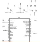
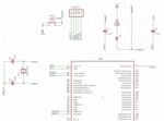
Please refer the image file.
PORTC and PORTD are connected with 7 SEGMENT(CC) display through 470R resistor and another two pins are used to drive an TRIAC(These not shown in the schematic).
My concept is when the switch S5 and S6 is turned ON means the LED have to glow and low state is given pic controller.But both LEDs are always in ON state,without operating the switch.I changed the PIC PINS state also but there is no change in LEDs,its always in ON STATE.

The TRIAC will be switched on based on the time interval.This is the basic operation of the circuit.At initial time the controller working fine,after sometimes(Nearly after 15MINS )there is no operation performed by the controller.It simply in idle state.

Please help to solve this issue..
 

Hi,

Why you have two 5V supplies?
* "+5V" for the PIC
* "+5V_l" for the LEDs
How are they generated, how are the related to each other? --> show the complete circuit.

One switch "NC" is wired and the other switch "NO" is wired. According this the "random"LED is "normally ON.
Maybe the switches are wrongly wired. --> check wiring.

Maybe the code is wrong. --> show us your code.

Klaus
 

Hi,

Why you have two 5V supplies?
* "+5V" for the PIC
* "+5V_l" for the LEDs
How are they generated, how are the related to each other? --> show the complete circuit.

Klaus

While using jumper pin in Eagle manually named the wire as like this.

- - - Updated - - -

Hi,


One switch "NC" is wired and the other switch "NO" is wired. According this the "random"LED is "normally ON.
Maybe the switches are wrongly wired. --> check wiring.


Klaus

For operating switch it is interchanged.If the random LED in ON position means their is no GND sensing given to the PIC controller.

- - - Updated - - -

Hi,

Why you have two 5V supplies?
* "+5V" for the PIC
* "+5V_l" for the LEDs
How are they generated, how are the related to each other? --> show the complete circuit.

One switch "NC" is wired and the other switch "NO" is wired. According this the "random"LED is "normally ON.
Maybe the switches are wrongly wired. --> check wiring.

Maybe the code is wrong. --> show us your code.

Klaus

Code:
#define	XTAL_FREQ	8MHZ		/* Crystal frequency in MHz */
#include "xc.h"
#include "pic16f877a.h"
#include "delay.h"

// CONFIG
#pragma config FOSC = HS        // Oscillator Selection bits (HS oscillator)
#pragma config WDTE = OFF       // Watchdog Timer Enable bit (WDT disabled)
#pragma config PWRTE = ON       // Power-up Timer Enable bit (PWRT enabled)
#pragma config BOREN = OFF      // Brown-out Reset Enable bit (BOR disabled)
#pragma config LVP = OFF        // Low-Voltage (Single-Supply) In-Circuit Serial Programming Enable bit (RB3 is digital I/O, HV on MCLR must be used for programming)
#pragma config CPD = OFF        // Data EEPROM Memory Code Protection bit (Data EEPROM code protection off)
#pragma config WRT = OFF        // Flash Program Memory Write Enable bits (Write protection off; all program memory may be written to by EECON control)
#pragma config CP = OFF         // Flash Program Memory Code Protection bit (Code protection off)


#define triac_1 RB2
#define triac_2 RB3 //outputs

#define change_value PORTDbits.RD5  //inputs

void System_init(void) {
    TRISA = 0b00001000;
    PORTA = 0b00001000;

    ADCON1 = 0XFF;
    CMCON = 0X07;

    TRISB = 0b00000010;
    PORTB = 0b00000010;

    TRISC = 0b00000000;
    PORTC = 0b00000000;

    TRISD = 0b01100000;
    PORTD = 0b01100000;

    TRISE = 0b00000010;
    PORTE = 0b00000010;

    ADCON1bits.PCFG0 = 0;
    ADCON1bits.PCFG1 = 1;
    ADCON1bits.PCFG2 = 1;
    ADCON1bits.PCFG3 = 0;
}

/**************************************************************
                    Main Program
 **************************************************************/
void main(void) {

    System_init();

    while (1) {
        triac_1 = 1;
        triac_2 = 0;
        DelayMs(200);
        triac_1 = 0;
        triac_2 = 1;
        DelayMs(200);

    }
}
 

You didn't show much on your circuit above regarding how reset circuitry and crystal are connected to the microcontroller.
 

Hi,

I see
* A ground symbol
* signals named with "GND"
* signals named with "GND_1"
--> Please use one solution only to prevent confusing us and yourself.

I see 6 "pieces" of signal named as "RESET".
--> Place the parts in useful groups and connect the signals directly.
(For sure this sometimes is not possible. But in your case it is.)

Klaus
jumper.jpg
jumper_2.jpg

Hai,in single side PCB,if there is an need of using jumper lead means i'm naming the wire after two leads of jumper in different name.
One side of the jumper lead is named as like the wire name in component and another based on where to connect the jumper lead.

I will practice to improve it...
If any tips available for using jumper lead means please guide.I will improve it surely.
 

Hi,

My advice:
Nowadays, with increasing swtiching frequencies, SMPS, Bluetooth, WiFi... and - especially because you need to be EMI / EMC compliant - I don´t think a single side PCB is useful anymore.
Don´t be surprised when a single sided PCB fails.

Use at least two sided. While one side should be GND only.

It´s more difficult to layout a reliably running single side PCB than a double side PCB.


Klaus

Hai,
Ok I will change to double side PCBs.

If using single side PCB means earthing the PCB will reduce the EMI/EMC issues..?
Or anyother way to reduce the EMI/EMC issues in single side PCB..?
 

Hi,

If using single side PCB means earthing the PCB will reduce the EMI/EMC issues..?
No.

Or anyother way to reduce the EMI/EMC issues in single side PCB..?
Advanced signal routing. As already said: it will be more complicated than with a double sided PCB.

PCB:
as already said:
Try to route all signals on one layer and the other layer is GND only.
This may not always be possible.

Before you give your PCB into production you may post your laoyut it here to be verified.

Klaus
 

Status
Not open for further replies.

Similar threads

Part and Inventory Search

Welcome to EDABoard.com

Sponsor

Back
Top