Simon_Chueh
Newbie level 3
Hello all,
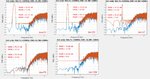
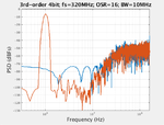
I am designing a CT-Delta Sigma ADC. The spec of this ADC is:
3rd-order, 4-bit Quantizer, Fs=320MHz, OSR=16, BW=10MHz, CIFF structure
The problem I encountered is some strange result from the FFT of the ADC. Attached figure is 5 different input bin; from low frequency to high frequency, with two different condition. One is with an ideal feedback current DAC which is generated from Verilog-A model, and the other one is with the current DAC in transistor level. Other block of the ADC in these two condition are all in transistor level.
I cannot explain and find out the reason that cause the noise floor getting high and even becoming flat or some strange ringing. 1 input which is bin=79 has the same result for both condition.
The attached result is from Spectre. I have tried Hspice, but the results are similar. The setting of Spectre transient that I use is:
moderate, gear2only, ++aps
FFT window is blackmanharris
I have already improve my current DAC but the results remain same. I don't know whether this is still the linearity problem of main feedback current DAC or not.
Hope anyone can give me some advice, I will be really appreciate!!