Continue to Site

Welcome to EDAboard.com

Welcome to our site! EDAboard.com is an international Electronics Discussion Forum focused on EDA software, circuits, schematics, books, theory, papers, asic, pld, 8051, DSP, Network, RF, Analog Design, PCB, Service Manuals... and a whole lot more! To participate you need to register. Registration is free. Click here to register now.

[ADS] Optimum settings for simulating spiral inductor

Status
Not open for further replies.

pragash

Advanced Member level 2
Joined
Jul 4, 2005
Messages
512
Helped
64
Reputation
128
Reaction score
59
Trophy points
1,308
Location
Oakland
Activity points
4,940
i have designed a filter with two spiral inductor in it for 2.5GHz application. When i simulate the whole layout with inductors in ADS (Momentum Microwave), the results didnt correlate with circuit simulation.

i re-simulated standalone inductor and compared the results with MSIND (TLines-Microstrip). No correlation between MSIND and the layout simulation so the problem is the spiral inductor.

i would like to know the optimum layout simulation settings for spiral inductor in order to obtain good correlation between MSIND and the layout. Take note that i have created the inductor from the MSIND so the layout simulation should correlate with circuit.

my spiral inductor (MSIND) is very compact. the parameters are:
N=17.7243
Ri=45.7773
W=9.75086
D=6.35643

im also thinking its not practical to simulate the whole layout together with the inductor using Momentum Microwave. its because its time consuming. its better to simulate the inductors separately and the connect them toegther in layout look-alike component. Please let me know your thought about this.

thanks.
 

Spiral inductors are sensitive to any solid ground plane below. They work much better (higher L at same geometry) if there is no ground plane. Have you modelled the same ground situation for circuit model and EM?

Separate simulation works if there is little coupling from the inductor to other parts of the circuit. That really depends on inductor size vs. substrate distance etc, so there is no universal rule.

To see what is wrong, have you compared the extracted L and R values?

What are the units for your numbers, is that mils? Can you show a layout screenhot?
 
Spiral inductors are sensitive to any solid ground plane below. They work much better (higher L at same geometry) if there is no ground plane. Have you modelled the same ground situation for circuit model and EM?

thanks. On my circuit simulation using MLIN and MSIND, i used PCB stackup with dielectric thickness (H) of 2.42mil. I assume i can have ground plane below. Do I need to remove the ground underneath all the way until Bottom Layer? If let's say I implement the inductor in the inner layer, does the ground plane above the inductor matters?

- - - Updated - - -

To see what is wrong, have you compared the extracted L and R values?
im comparing L value with the MSIND. i compare R as well.

- - - Updated - - -

What are the units for your numbers, is that mils?

units are in mils

- - - Updated - - -

Can you show a layout screenhot?

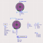
sure. i have attached the pictures here. inductor simulation results.png

- - - Updated - - -

inductor simulation.png

another picture is here.

- - - Updated - - -

port is the MSIND inductor (reference). im trying to match layout spiral (Port 1 and Port 3) to port 2.

- - - Updated - - -

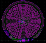
inductor layout.png

layout simulation of a standalone inductor

- - - Updated - - -

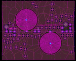
complete layout.png

layout simulation of a complete layout together with two spiral inductor.

- - - Updated - - -

there is a problem in completely removing all the ground plane underneath of the inductor. the inductor is grounded at the middle/center. if i strip all the ground off, the inductor ground will be floating!
 

Reff simulation unable to match the value of MSIND. MSIND giving consistant Reff = 0ohm across the frequency band whereas, layout is giving 12 to 50ohm. do you have any idea on this problem?
 

thanks. On my circuit simulation using MLIN and MSIND, i used PCB stackup with dielectric thickness (H) of 2.42mil. I assume i can have ground plane below. Do I need to remove the ground underneath all the way until Bottom Layer? If let's say I implement the inductor in the inner layer, does the ground plane above the inductor matters?

Any ground matter above/below matters, and reduces inductance a lot. Keep the inductor area (plus some extra margin) clear from other metal than changes the inductor's magnetic field.

there is a problem in completely removing all the ground plane underneath of the inductor. the inductor is grounded at the middle/center. if i strip all the ground off, the inductor ground will be floating!

I meant a solid metal area where eddy currents can flow. An underpass line for connection is not a problem at all.

~~

I see two reasons for major differences of results:
1) The closed metal loop around the inductor also has a strong effect: your inductor becomes a transformer with a shorted secondary. This is only seen in EM because you don't have the metal frame in the schematic model.
2) There is no metal loss included in your schematic model, you have almost perfect conductor in your MSUB block (cond = 1E50S/m).

~~

Sidenote: Your layout with the very small inner hole is inefficient. I think will get better Q factor if you have some reasonable inner diameter, one third of outer diameter or so.
 
Last edited:
thank you very much for the comments. i have few questions.

- - - Updated - - -

I see two reasons for major differences of results:
1) The closed metal loop around the inductor also has a strong effect: your inductor becomes a transformer with a shorted secondary. This is only seen in EM because you don't have the metal frame in the schematic model.

what is the minimum distance between inductor and the metal ground on the top layer?

- - - Updated - - -

Sidenote: Your layout with the very small inner hole is inefficient. I think will get better Q factor if you have some reasonable inner diameter, one-third of outer diameter or so.

are you talking about Via hole? i will try to increase the via dimension. i also know that two vias are better than single via. just that i dont have space..
 

what is the minimum distance between inductor and the metal ground on the top layer?

A spacing of 0.5 inductor diameters on each side would be fine, then the ground has little effect. If you make it smaller, you will see a decrease in inductance and increased losses. If you can afford that, you can make the spacing smaller -- but model it in EM to see how much it changes.

are you talking about Via hole?

No, I am talking about the diameter of the innermost turn. Making that so very small, as you did, results in poor inductor performance. I would make the inner turn no smaller than 1/3 of the outer diameter.
 
thank you very much for useful suggestions

- - - Updated - - -

i will place the inductor in the inner layer so it can have maximum ground clearance to the adjacent ground.

- - - Updated - - -

No, I am talking about the diameter of the innermost turn. Making that so very small, as you did, results in poor inductor performance. I would make the inner turn no smaller than 1/3 of the outer diameter.

actually, the coil has uniform diameter across the spiral. i don't have a different diameter for inner turns vs outer turns.
 

i think i get what u mean now. you taking about Ri of MSIND which is Inner radius measured to the center of the conductor.
 

i think i get what u mean now. you taking about Ri of MSIND which is Inner radius measured to the center of the conductor.

Yes, exactly.

The inductor creates a magnetic field around the traces. In your layout, the few innermost turns don't add much inductance because the opposite fields from the "other side" are very close, and both fields cancel. The major effect from the innermost turns is: more series resistance. If you re-design the inductor with a center hole, the Q factor will be better.

Not sure if that matters for your design - for filters the Q matters, for chokes we don't care.
 
im designing filter so Q is important to have high Q so that the Reff will be very low. thank you for your advice.
 

Status
Not open for further replies.

Part and Inventory Search

Welcome to EDABoard.com

Sponsor

Back
Top