F
fourtytwo
Guest
My wife kept saying my malfunctioning circuit sounded like a rattlesnake, well her hearing is a might higher pitched than mine but sure enough the main transformer of my half bridge kept saturating, fortunately the overcurrent detector was shutting it down before any serious damage but what was the cause ? I investigated dozens of circuit nodes with the scope, some harder than others due to the voltages involved. Eventually I discovered the high-side was unaccountably shutting down meaning the transformer went out of balance and the following low side period the transformer went into saturation. My mind leapt to high side UVLO, now this is a real beast to prove as not only are all the signals switching but they have a huge voltage swing so seeing a volt or so difference to determine if the UVLO threshold is being tripped is hard indeed, to be sure I replaced the boost components and increased the chips supply voltage neither of which fixed the problem! Then I got to thinking of switching transients upsetting the substrate bias but nope nothing exceeded the chip spec Hmmmmm
I should mention due to a previous failure of the entire half bridge that took the driver out I had replaced both mosfets and the driver chip, I decided to also up the latter from a 2110 to a 2113 to maybe save it the next time around but otherwise the circuit, pcb and all was identical to when everything had been working normally.
In order to probe the actual chip pins more closely I fitted a chip-clip and the problem went away!! Needless to say I thought this was crazy so repeated the test several times but it remained ok with chip clip on, bad with off! (Way back in the 70's this would often happen with high speed logic and there used to be a standing joke about shipping pcb's to the customer with chip-clips in place to ensure it worked).
So a few pF somewhere fixes something! Then it struck me the input pins were the highest impedance and the SD pin is not used in this design and left floating (well there is a so-called internal pulldown) however when the pin was hard grounded the fault went away chip-clip on or off Phew!! Interestingly with the old chip this had not been a problem.
The date codes of both chips were the same (713P). The funny thing is there appeared to be no effect on the low-side driver at all and that's what initially led me to ignore the SD pin, anyway peeps don't leave it floating if your not using it as suggested in the data sheet, even just a pin with nothing connected to the pad gets enough pickup in a high dv/dt environment to cause mysterious trouble.
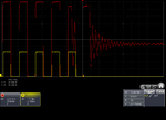
The scope shot shows yellow HIN red HO, so normally the waveform is as expected until the high side unexpectedly does not turn on at all (remember this waveform also includes transformer primary ringing) but the low side continues to operate normally. The trigger point is the primary overcurrent signal that shuts everything down (fortunately as I have blown tracks off the pcb several times when this part failed)!
I should mention due to a previous failure of the entire half bridge that took the driver out I had replaced both mosfets and the driver chip, I decided to also up the latter from a 2110 to a 2113 to maybe save it the next time around but otherwise the circuit, pcb and all was identical to when everything had been working normally.
In order to probe the actual chip pins more closely I fitted a chip-clip and the problem went away!! Needless to say I thought this was crazy so repeated the test several times but it remained ok with chip clip on, bad with off! (Way back in the 70's this would often happen with high speed logic and there used to be a standing joke about shipping pcb's to the customer with chip-clips in place to ensure it worked).
So a few pF somewhere fixes something! Then it struck me the input pins were the highest impedance and the SD pin is not used in this design and left floating (well there is a so-called internal pulldown) however when the pin was hard grounded the fault went away chip-clip on or off Phew!! Interestingly with the old chip this had not been a problem.
The date codes of both chips were the same (713P). The funny thing is there appeared to be no effect on the low-side driver at all and that's what initially led me to ignore the SD pin, anyway peeps don't leave it floating if your not using it as suggested in the data sheet, even just a pin with nothing connected to the pad gets enough pickup in a high dv/dt environment to cause mysterious trouble.
The scope shot shows yellow HIN red HO, so normally the waveform is as expected until the high side unexpectedly does not turn on at all (remember this waveform also includes transformer primary ringing) but the low side continues to operate normally. The trigger point is the primary overcurrent signal that shuts everything down (fortunately as I have blown tracks off the pcb several times when this part failed)!
Attachments
Last edited by a moderator:
")