Continue to Site

Welcome to EDAboard.com

Welcome to our site! EDAboard.com is an international Electronics Discussion Forum focused on EDA software, circuits, schematics, books, theory, papers, asic, pld, 8051, DSP, Network, RF, Analog Design, PCB, Service Manuals... and a whole lot more! To participate you need to register. Registration is free. Click here to register now.

How to generate EM simulation on ADS so that it interacts with the transistor model?

Status
Not open for further replies.

skatefast08

Full Member level 3
Joined
Jan 24, 2018
Messages
189
Helped
2
Reputation
4
Reaction score
2
Trophy points
18
Activity points
1,779
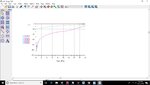
ok, I tried to so many different ways to create an EM simulation so that I can get an approximate s-parameter simulation as in the schematic as shown below in the figure 1 that corresponds to the s-parameter graph in figure 2. In the layout, I used 4 different conductors (ex. M2, cond, cond2, M3) to represent different pins on the transistor (ex. G, S1, S2, and D). Also, I created 4 vias, 2 on the S1, and 2 on the S2 as shown in my layout. The layout is shown in Figure 3. For my s-parameter simulation of the layout is shown in figure 4. What am I doing wrong? I have shown my substrate as shown in figure 5. I also show another pic in figure 6 if that helps, because I get a warning during simulation.

My main task is to simulate a layout that can give me a good representation of what I have in figure 2. I want to map the ADS-transistor-model from the schematic window to the layout and then be able to generate the new s-parameters based on the whole layout. Is this the way to do it, or how would you do this? I want to simulate my LNA design on EM simulation, but I want to start out with the basics with just the transistor itself. thanks!

ATF55143(50OHM_Terminations).png
figure 1

sparamgraph.png
figure 2

mapped_pins_from_schematic.png
figure 3

s-param_from_layout.png
figure 4

substrate.png
figure 5

other_pics(1).png
figure 6
 

Attachments

  • sparam_graph.jpg
    sparam_graph.jpg
    74.6 KB · Views: 168
Last edited:

You have lack of experience on RF Simulations..( Read and search lot..)
I recommend you to design a PCB in a PCB Design program by inspiring from App. Notes of that transistor then obtain Gerber Output after that Import this file onto ADS then do your EM simulations.
This is most practical way to do that.Otherwise you will confuse all and you won't never figure them out..
 
Doing a simple s-parameter test on 1 single transistor should not be that difficult. How difficult is that? How would you do this? I'm just trying to figure out this one specific task. I was never taught how to use ADS, and I figured out a lot about it. I also programmed my own RF simulator on MATLAB to design an LNA that is just like how ADS simulates an ideal LNA circuit, you don't think I understand some stuff on here? If I was the programmer for ADS, of course I would know how to do this specific task I'm trying to do. If I was to design my own program to do this procedure, I would have the actual ADS-model interact with the layout. Isn't the layout only about the dimensions and material?
 
Last edited:

If you don't want to spend the money on ADS training (payed), study the examples that come with ADS.

One mistake is your EM stackup. For your setup, you need to set explicit ground pins for each port on the drawn bottom metal.

As a beginner, start with an infinite ground at the bottom side. Then, it is enough to just place the signal (+) pin at the top metal layer.
 
How come for every EM simulation I do with a transistor, I don't get any gain higher than 0 during EM simulation and no resemblance in s-parameter graphs? I biased the transistor correctly in the ADS schematic and it simulates perfectly, but when im specifying the pins on the transistor from the ADS layout, I don't get any accurate s-parameter simulation. why?

Later I decided not to use vias, a ground plane, or even the bias network anymore. I am making everything as simple as possible with and just wiring the source pins to ground, the gate for port 1, and the drain for port 2. I am using the SOT343 model (which goes with the ATF55143 transistor) and still no close approximations in s-parameter simulations, why? I put my pins in the correct order as the schematic to the layout and no progress has been made.
 
Last edited:

Status
Not open for further replies.

Part and Inventory Search

Welcome to EDABoard.com

Sponsor

Back
Top