Continue to Site

Welcome to EDAboard.com

Welcome to our site! EDAboard.com is an international Electronics Discussion Forum focused on EDA software, circuits, schematics, books, theory, papers, asic, pld, 8051, DSP, Network, RF, Analog Design, PCB, Service Manuals... and a whole lot more! To participate you need to register. Registration is free. Click here to register now.

DAC design (input signal)

Status
Not open for further replies.

AllenD

Member level 5
Joined
Aug 7, 2017
Messages
91
Helped
0
Reputation
0
Reaction score
0
Trophy points
6
Activity points
1,193
Hi Team
I have a question about DAC design.

1. So for a DAC, what is the input waveform should look like?
A) A true digital signal, eg, made of "011001" B) A quintized analog signal, eg, the output of a ADC?

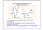
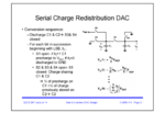
2. I assume the answer to the 1st question is "A", then, let's say I have a DAC using R2R Binary Ladder, are the input of the DAC(V1-V4)
A) Arrive at the same time B) Arrive one by one in the time domain.

Thanks
Allen
 

Attachments

  • Screenshot from 2018-12-07 00-06-11.png
    Screenshot from 2018-12-07 00-06-11.png
    145.3 KB · Views: 118
  • Screenshot from 2018-12-07 00-08-15.png
    Screenshot from 2018-12-07 00-08-15.png
    161.2 KB · Views: 108

Hi,

In my eyes: If you want to design a DAC, you should get/have/decide the specification first.
It needs to tell you about
* the interface (signal levels, timing, serial, parallel, differential...)
* the DAC type (R2R, Delta Sigma, resolution,....)
* and the electrical specifications of the analog signal (voltage, current, levels, noise, timing, accuracy, INL, DNL ...)

If you have this specification, all the questions above should be answered.

To the questions in detail:
1) The usual signal to a DAC is a binary signal with logic levels. Your question whether A or B more sounds if the bits come as serial datastream or parallel. Both is usual. Serial may be: I2C, SPI, I2S, LVDS ....They may come in single ended as well as differential.

2) Now think about it as serial...one bit after the other. If now comes the first bit of a dataword...what do you think should happen to this bit at the R2R dac ... and what shoukd happen to all the other bits of the R2R DAC (should they keevp previous state or start with a preset value? And now think how the analog output will look like (in time, bit after bit) when this happens.
(As so often I recommend to use a sheet of paper and a pencil or any software (even Excel will do) to "simulate" your idea.
No need for exact timing or exact voltage levels ... )

I assume (independent of the scenario you think about) this will not give satisfying analog output.
Thus I see only two meaningful solutions:
* update all digital inputs to a R2R ladder at the same time (preferred. Simple shift register)
* or use an analog "hold" circuit at the analog output

Klaus
 

Hi,

* or use an analog "hold" circuit at the analog output

Klaus

Hi Klaus,
Thanks for helping me! You answer is very inspiring!
As you suggested, I tried to simulate the "serial charge redistribution DAC" as in the first pic I attached earlier.But I am facing some problem with how to "hold" the output. The output is the voltage created by the charge stored in the cap C2. I tried to use a simple "switch+C" as the sample and hold, but this will act as a negative gain since the charges will only be partially transferred.
Can you please let me know what exactly is the "analog "hold" circuit" you are referring to? a unity gain buffer? a integrator circuit that make sure all the charges are moved from C2 to the feedback cap?

Thanks
Allen
 

Hi,

Do an internet search for "sample and hold circuit".

Klaus
 

Status
Not open for further replies.

Similar threads

Part and Inventory Search

Welcome to EDABoard.com

Sponsor

Back
Top