Continue to Site

Welcome to EDAboard.com

Welcome to our site! EDAboard.com is an international Electronics Discussion Forum focused on EDA software, circuits, schematics, books, theory, papers, asic, pld, 8051, DSP, Network, RF, Analog Design, PCB, Service Manuals... and a whole lot more! To participate you need to register. Registration is free. Click here to register now.

IR2110 driver output causing shoothrough despite deadtime

Status
Not open for further replies.

RBN44

Newbie level 2
Joined
Nov 2, 2017
Messages
2
Helped
0
Reputation
0
Reaction score
0
Trophy points
1
Activity points
21
Hi, I'm having trouble with the ir2110 output. I'm working on a class d full bridge amplifier and I use 2 ir2110 to drive 4 irf540N mosfets. The switching frequency I use to generate the PWM is 240kHz and I include a 100ns deda-time (ideally would be no more than 50ns), but still got some peak in the output that generates shoothrough. In the picture you can see the circuit, that includes a snubber, the filter and load.
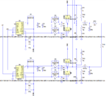
ir2110_circuit.PNG

The porblem I need help with is that the deadtime is correct at the input of the ir2110, but in the output i get a peak (circled in red) which is causing the problem and I don't know what causes it.

ir2110_input_output.PNG

Thanks in advance.
 

Gate voltage rising to 3 V doesn't mean shoot-through with IRF540. If you feel that the gate voltage isn't fully turned off before activating the other transistor, you would increase the dead time.

Oscillating rising edge is a different thing, I guess is caused by parasitic circuit inductance.
 

22uF as bootstrap is overkill for IRF540. 100 nF is fine.

Voltage is clamped at ~3V. You might decrease the clamp voltage via using a Schottky diode e.g. 1N581x. Or increase dead time to eliminate it altogether.

get a peak (circled in red)
The peak is due to the charging characteristic of the gate of a non ZVS switching transition.

- - - Updated - - -

Oscillating rising edge is a different thing, I guess is caused by parasitic circuit inductance.
Can't see any modeled lumped parasitic inductance in the simulated circuit. Real life would. Therefore I am a bit surprised by that oscillation since it does not look exactly like usual gate characteristics.
I think oscillation occurs when the GS voltage hits the supply voltage if there was a parasitic inductance.
 
Last edited:

It's definitely not completely off, I get 60A peaks of around 20ns duration.

ir2110_shootthrough.PNG
 

Hi,

It might be reverse recovery of your diodes.

And I agree with CataM about the bootstrap capacitor. I don't think the 22uF brings any benefit....especially at 240kHz.

Klaus
 

In fact the wrong 22uF could really cause problems at the
edges, if ESL, ESR are too high. A lonely electrolytic or low
quality tantalum could be like that. A decent HF 1uF or 0.1uF
might be a good supplement.

The "spikes" I think may just be Miller plateau plus some
setup ringing, are you sure the chosen FET is small enough
(Cgd in particular) that IR2110 is really suitable?
 

The waveforms are apparently Ltspice simulation results. Parameters like capacitor ESR are hardly modelled.

If the transistor model includes terminal inductance or realistic voltage dependent junction capacitances - we don't know.
 

Status
Not open for further replies.

Similar threads

Part and Inventory Search

Welcome to EDABoard.com

Sponsor

Back
Top