Continue to Site

Welcome to EDAboard.com

Welcome to our site! EDAboard.com is an international Electronics Discussion Forum focused on EDA software, circuits, schematics, books, theory, papers, asic, pld, 8051, DSP, Network, RF, Analog Design, PCB, Service Manuals... and a whole lot more! To participate you need to register. Registration is free. Click here to register now.

Create ground plane multi layers in Eagle

Status
Not open for further replies.

bob2987

Junior Member level 1
Joined
Feb 20, 2014
Messages
18
Helped
0
Reputation
0
Reaction score
0
Trophy points
1
Activity points
192
Hi,

I would like to create a ground plane between 2 wires (on the top), i have a layer for the ground and i would like to associate this ground plane on the top to the ground layer.

When i changed the the name of the ground plane (GND) , it dissapears, i thought about a via to change the layer from the top layer.

Thank you.
 

Hi,

I think I could help you, but I'm confused...I don't know what and how you need.

Show a picture. Even hand drawn is OK.

I would like to create a ground plane between 2 wires (on the top)
Although possible, it's not usual. Tell us why.

, i have a layer for the ground and i would like to associate this ground plane on the top to the ground layer.
If you have a GND plane (on which layer?), why do you need another one?
I assume the existing GND plane is a polygon with the according signal name...the same you can do at every layer.

When i changed the the name of the ground plane (GND) , it dissapears, i
It dissapears when there is no such signal inside this area. But why did you change the name?
And do you know about "ratsnest".

Did you go through the EAGLE tutorials...and other tutorials in the internet?

i thought about a via to change the layer from the top layer.
Don't know what this means....

Klaus
 

ground_plane.png

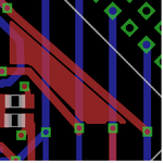
Hi, as you can see on the image there is a red area which is between 2 wires. This area is connected to anything. My GND plane is the third one. I did this to prevent to the crosstalk between the 2 signals.

Thank you.
 

Hi,

This is no GND plane. This is just copper pour. It is not connected to anything as far as I can see.

I don´t see a GND plane. You talk about "third one"... What does this mean? A third layer? Then is surely has a number, a name (both should be used to avoid confusion) and can be made visible.

*****
Still unsure what you want to do:
If you want it to be GND, then you need to add any connection.
* This can be a WIRE on the TOP LAYER from any GND signal to this POLYGON.
* or you can use a VIA to get a GND connection from any other LAYER. This via needs to be NAMEd like the GND signal name.

In either case: the POLYGON on the TOP layer needs to have the same NAME as the according signal.

***
For reducing cross talk you could just draw a WIRE instead of the polygon.
But I doubt that this wire or pologon will result in much improvement with the given layout.

Klaus
 

Status
Not open for further replies.

Part and Inventory Search

Welcome to EDABoard.com

Sponsor

Back
Top