T
treez
Guest
Hello,
What are the chances of getting arcing between in-line TO220 pads on a 60W Offline Flyback SMPS FET. (FR4 PCB coated with solder resist)
Our contractor has designed a 60W offline (240VAC) Flyback LED driver (PFC’d) for us. It is for outdoor use.
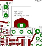
The footprint for the TO220 primary FET is just three PTH pads in a line, ie, no bending out of the middle leg of the TO220 to facilitate greater clearance between the Drain pad and the other two pads. The PCB is not conformal coated, but just normal solder resist coated.
There is just 0.7mm of clearance between drain pad copper and source/gate pad copper.
The PCB Enclosure is plastic, and “snap-fit”, …in other words, it has “seam” lines through which moisture laden air could enter the PCB enclosure.
The PCB enclosure will sit inside an aluminium enclosure, which does have a rubber gasket around its closure-contact surfaces….so I suppose this is some surety that moisture laden air will not enter into the aluminium outer enclosure…however, we believe that moisture can actually “breathe” through such rubber seals?
Anyway, do you think that the 0.7mm clearance between the drain pad and other pads will cause problems due to moisture ingress? We are going to do a test whereby we spray a film of water over the TO220 footprint, and then power up the LED driver. However, we wonder if tap water is going to give a realistic indication of whatever the atmospheric moisture might be like?
We don’t want a footprint where the drain pad is bent out, because its an extra assembly cost.
What will happen in our “sprayed tap water” test, and will it be realistic to what real atmospheric moisture will be like?
Thread #19 of the following says that arcing is a possibility between the pads, but how likely is this in reality?...
https://www.edaboard.com/showthread...FET-and-legs-not-bent-Too-close-to-each-other
…according to this, the TO220 leg spacing on the body of the TO220 is insufficient to meet standards, and so flashover may occur here?...in this case, this means that it would be a waste of time to bend out the middle (drain) leg of the TO220.
Post #10 of the following shows a good way to maximise the clearance between in-line TO220 pads….
https://www.edaboard.com/showthread...learance-between-drain-and-source-pads-on-PCB
What are the chances of getting arcing between in-line TO220 pads on a 60W Offline Flyback SMPS FET. (FR4 PCB coated with solder resist)
Our contractor has designed a 60W offline (240VAC) Flyback LED driver (PFC’d) for us. It is for outdoor use.
The footprint for the TO220 primary FET is just three PTH pads in a line, ie, no bending out of the middle leg of the TO220 to facilitate greater clearance between the Drain pad and the other two pads. The PCB is not conformal coated, but just normal solder resist coated.
There is just 0.7mm of clearance between drain pad copper and source/gate pad copper.
The PCB Enclosure is plastic, and “snap-fit”, …in other words, it has “seam” lines through which moisture laden air could enter the PCB enclosure.
The PCB enclosure will sit inside an aluminium enclosure, which does have a rubber gasket around its closure-contact surfaces….so I suppose this is some surety that moisture laden air will not enter into the aluminium outer enclosure…however, we believe that moisture can actually “breathe” through such rubber seals?
Anyway, do you think that the 0.7mm clearance between the drain pad and other pads will cause problems due to moisture ingress? We are going to do a test whereby we spray a film of water over the TO220 footprint, and then power up the LED driver. However, we wonder if tap water is going to give a realistic indication of whatever the atmospheric moisture might be like?
We don’t want a footprint where the drain pad is bent out, because its an extra assembly cost.
What will happen in our “sprayed tap water” test, and will it be realistic to what real atmospheric moisture will be like?
Thread #19 of the following says that arcing is a possibility between the pads, but how likely is this in reality?...
https://www.edaboard.com/showthread...FET-and-legs-not-bent-Too-close-to-each-other
…according to this, the TO220 leg spacing on the body of the TO220 is insufficient to meet standards, and so flashover may occur here?...in this case, this means that it would be a waste of time to bend out the middle (drain) leg of the TO220.
Post #10 of the following shows a good way to maximise the clearance between in-line TO220 pads….
https://www.edaboard.com/showthread...learance-between-drain-and-source-pads-on-PCB