Continue to Site

Welcome to EDAboard.com

Welcome to our site! EDAboard.com is an international Electronics Discussion Forum focused on EDA software, circuits, schematics, books, theory, papers, asic, pld, 8051, DSP, Network, RF, Analog Design, PCB, Service Manuals... and a whole lot more! To participate you need to register. Registration is free. Click here to register now.

BJT transistor mextram model accuracy

Status
Not open for further replies.

inass57

Member level 2
Joined
Jan 18, 2018
Messages
48
Helped
1
Reputation
2
Reaction score
1
Trophy points
8
Activity points
431
Hi guys!

I've been trying to design an LNA using BJT transistor, on the first try the results of my simulations and measurements were different and i concluded that it must have been related to the permittivity of the substrate (i had a resonator on the board) . so i redesigned the LNA using the correct permittivity this time but still no luck.

So i was wondering how accurate the transistor model is actually? and if they are not 100% accurate how does a person design correctly their amplifier?

I'm working at 10GHz.

Thank you in advance.
 
Last edited:
Mextram model is a very accurate BJT model.There might be some other additional effects..
 

If you take a look at this application note provided by NXP on their BFU730F, you'll see that they don't have the same results as their simulation:
https://www.nxp.com/docs/en/application-note/AN11010.pdf

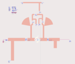
My design is as shown below: for the capacitors on the RF line i used the capacitor model to be as close to reality as possible.
The frequency shift in my measurments is about 300MHZ for S11 and 400MHz for S22, while i can try to make it work by cutting the stubs a little, changing the capacitors etc i fear the repeatability of such a procedure since it'll be handmade.

Capture,;,.PNG
 

Have you ever simulated your PCB layout(Momentum)+Circuit Schematic in ADS ??
Plus, your layout is not same as NXP's in App. Notes.If your operating frequency is really high ( I think Ku Band ) every detail will be very important including the models of
passive components.I recommend you to use "real measured models" ( Modelithics ) for passive components, not approximated models.They change too much everything..
Sheet filters impact very much the frequency response, don't forget.If you measure the NF of this amplifier, you will -possibly- far away from desired point.
Substrate's parameters accuracy are also important.
Decoupling capacitors ( C5,C6) are very bad placed, follow up the NXP's layout recommendation.
I have worked with Mextram models many years for RFIC circuits, they are really accurate.
 
  • Like
Reactions: ktr

    ktr

    Points: 2
    Helpful Answer Positive Rating
Yes, my simulations are Layout+schematics:
The capacitors C1/C2/C3/C4 are simulated using the model provided by murata however the other components are ideal componenets during the simulation as they are LF components used just for biasing and the RF signal doesn't go there because of the bias T. is there something that i'm missing?

Why do u say that C5 and C6 are badly placed? and what recommendations do you suggest?

and i'm sorry i don't understand what you mean by sheet filter.....
For the substrate, i'm simulating using the right permittivity as the resonator is working at the wanted frequency.

Thank you so much for your time, i really appreciate it.

Capture,;,.PNG
 

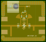
-Your layout does not cover Emitter GND connection VIAS.This is important because these vias might be a part of matching.
-C5 and C6 ( decoupling capacitors) are pretty far from Biasing resistors, you should place them very close to the resistors with a strong tied GND connections.
-GND connections of those capacitors are ideal but it's a mistake because there is too much difference between ideal GND and through VIA GND.This can be a part of fine tuning of the amplifier
-How you have obtained the Noise Matching circuit ?? It is seemingly not a proper circuit.
-Does Schematic Version of this amplifier work well ?? If it doesn't, you should review your circuit.(The schematic version must be very well modeled)
 

NXP didn't use radial stubs, just rectangular microstrip capacitors, but seems that everything works fine (BW about 2GHz for S11/S22 < -10dB, and even greater (3GHz) for the gain S21 >10dB).
Radial stubs works fine, until they are wrong placed on the PCB. Sometime a rectangular strip capacitor will work better than a radial stub.

If you look to the NXP layout you will see small matching stubs just near the transistor.
In your PCB, because the matching stubs are far away from the transistor, actually you are not doing impedance (or noise) matching for the transistor, but for the long inp/output transmission lines.

NXP layout is much more compact (very short traces) for the RC network placed after the stability resistors (R1, R2 in their design).
 

I recommend you to use "real measured models" ( Modelithics ) for passive components, not approximated models.They change too much everything..
I have worked with Mextram models many years for RFIC circuits, they are really accurate.

BigBoss, regarding this "real measured models". What should I do to get this?
 

Radial stubs works fine, until they are wrong placed on the PCB. Sometime a rectangular strip capacitor will work better than a radial stub.

When do you know it's wrongly placed?

If you look to the NXP layout you will see small matching stubs just near the transistor.
In your PCB, because the matching stubs are far away from the transistor, actually you are not doing impedance (or noise) matching for the transistor, but for the long inp/output transmission lines.
you mean i sould be matching before the bias T and the DC block? why does the way i did it work on simulation but not in real life?

NXP layout is much more compact (very short traces) for the RC network placed after the stability resistors (R1, R2 in their design).
would that be relevant if the bias T doesnt do its work ot in all cases?

- - - Updated - - -

-Your layout does not cover Emitter GND connection VIAS.This is important because these vias might be a part of matching.
How do i do that? by putting pins on the vias during EM simulations?

-How you have obtained the Noise Matching circuit ?? It is seemingly not a proper circuit.
I put the transistor between the two bias T and DC blocks from each side, then using the S parameters i traced the gain and noise circles, i choose the input impedance and used the smith chart tool in ADS to match, afterwards i matched the output impedance to 50OHm (this usualy mismatch the imput but i do some tuning to get to the desired level)

-Does Schematic Version of this amplifier work well ?? If it doesn't, you should review your circuit.(The schematic version must be very well modeled)
after the schematic simulation and moving to the EM simulation i had to do some tuning....;but i thought that was normal, is it not?
 

NXP didn't use radial stubs, just rectangular microstrip capacitors, but seems that everything works fine (BW about 2GHz for S11/S22 < -10dB, and even greater (3GHz) for the gain S21 >10dB).

But if you compare their simulation to the mesurements, it's not the same thing, which is the problem i'm facing...
 

Status
Not open for further replies.

Part and Inventory Search

Welcome to EDABoard.com

Sponsor

Back
Top