Continue to Site

Welcome to EDAboard.com

Welcome to our site! EDAboard.com is an international Electronics Discussion Forum focused on EDA software, circuits, schematics, books, theory, papers, asic, pld, 8051, DSP, Network, RF, Analog Design, PCB, Service Manuals... and a whole lot more! To participate you need to register. Registration is free. Click here to register now.

Can LM3914 be set up to work as an exclamation point and alarm flasher?

Status
Not open for further replies.

SparkyChem

Member level 3
Joined
Apr 22, 2010
Messages
57
Helped
0
Reputation
0
Reaction score
0
Trophy points
1,286
Location
Lima, Peru
Activity points
2,084
As the title implies I'm trying to make LM3914 to work as an exclamation point and alarm flasher. There is already a set up how to achieve both individually in the documentation from the LED bar driver. However I am confused at how to make it work for my needs based the parameters explained below.

My requirement needs to work with an input going from -5V to +5V, indicating over range for both. i.e lets say if the input is -6V, the bar indicator has to begin with the "center at zero" and to flash as indicate over range and the same for +5V thus if +6V turning on the leds from zero and flashing to indicate again over range. So How can I build an indicator with those parameters? :thinker:

I think it has something to do with appending these recommended circuits but I don't know how to do that or if that is the best way to go.

GQVCer7.png

In the documentation referring to exclamation point there is a 3V pulse going in the input through the base of the transistor and it recommends that very specific voltage. However I don't have it available. Can 5V be used instead?. What modification should be made on that part?

I tried to inspect all sources for trying to answer my question or show my progress if this can be done, but I couldn't find anything conclusive. Therefore can somebody with more experience than me help me with this matter?.

Btw please don't say you can do that with a microcontroller or some other IC, I'm aware that there are other methods but that is not what I'm looking for as my needs require specific use of the LM3914.
 

Hi,

In the documentation referring to exclamation point there is a 3V pulse going in the input through the base of the transistor and it recommends that very specific voltage. However I don't have it available. Can 5V be used instead?. What modification should be made on that part?
It's just Ohm's law.

Think about this:
1)
For a raw estimation you could say the 1.5kOhms resistor limits current at 3V to 2mA.
It should be no problem for you to calculate the resistor value that does the same for a 5V signal?

2)
For a more precise calculation you may consider that V_BE_ON is about 0.6V.
If you now use Ohm's law you will get a more close operating situation for the bjt.

3)
Use Ohm's law to calculate the current through the 1.5k Ohms resistor with 5V input signal.
Then read the bjt's datasheet whether the bjt can handle this base current.


Klaus
 

As Klaus mentions, it is only related to re-calculating base resistor values.

That particular transistor all that does is to fully discharge the capacitor that had been previously charged with the signal voltage.
After the base drive is released, the capacitor will recharge again.

The resulting display really grabs your attention.

For all that matters, the bipolar transistor could even be replaced with a small signal Mosfet, like the 2N7000
 

Hi,


It's just Ohm's law.

Think about this:
1)
For a raw estimation you could say the 1.5kOhms resistor limits current at 3V to 2mA.
It should be no problem for you to calculate the resistor value that does the same for a 5V signal?

2)
For a more precise calculation you may consider that V_BE_ON is about 0.6V.
If you now use Ohm's law you will get a more close operating situation for the bjt.

3)
Use Ohm's law to calculate the current through the 1.5k Ohms resistor with 5V input signal.
Then read the bjt's datasheet whether the bjt can handle this base current.


Klaus

Supposing that the transistor that I intent to use is a 2N3904 looking at the datasheet mentions, (see 2N3904 ) the collector current is 200 mA. Therefore by doing some circuit analysis (see figure from below),

igkaQZz.png


Because laTex seems not functioning properly in the forum I had to resort to other ways to display the equations needed.

fZI1TSL.png]


In short (unless I did overlooked anything what I found is that 19 ohms can be used for both resistors to get around 200 mA) but because this value means is the maximum boundary for which the base can resist I think 1 kOhm can be safe to go. Not sure if this is the right calculations.

Yet this doesn't answer the main question which is how can I make the LM3914 to work as the desired specifications, to act as an exclamation point and an alarm flasher in a symmetrical input?!.

- - - Updated - - -

As Klaus mentions, it is only related to re-calculating base resistor values.

That particular transistor all that does is to fully discharge the capacitor that had been previously charged with the signal voltage.
After the base drive is released, the capacitor will recharge again.

The resulting display really grabs your attention.

For all that matters, the bipolar transistor could even be replaced with a small signal Mosfet, like the 2N7000

In my previous reply, I mentioned that I intend to use 2N3904 however it looks that 2N7000 might be a better choice, but still the main question has not been answered I hoped that somebody could help me to address that necessity, since that is the core of my problem.
 

Hi,

I haven't thought this through fully but to give a rough idea, could you use a non-inverting OA (for the +5V) and an inverting OA (for -5V) type of circuit and feed their signals into a single supply device, maybe a non-inverting summing OA, which is used as the input device to the LM3914?

I recommend having a good browse through op amp application notes for similar circuits, maybe a pos/neg peak detector could work. As far as I can see, you'll need a level shifter on a dual supply for the negative range to make the output polarity positive.
 

Hi,

the collector current is 200 mA
Your calculation.
I3 goes to the base, thus you need to look formax base current, but you said collector current.
but max base current is just to check if it can withstand the increased (5V instead of 3V) base current.
You don't go to the limit.
When you calculate with base current on a switching (saturated) bjt, then you should consider I_base = I_collector / 10.
Where I_collector is the max expectable load current and not the maximum limit.

Sadly I have no experience with LM3914, thus I can't help you with that.

Klaus
 

Hi,


Your calculation.
I3 goes to the base, thus you need to look formax base current, but you said collector current.
but max base current is just to check if it can withstand the increased (5V instead of 3V) base current.
You don't go to the limit.
When you calculate with base current on a switching (saturated) bjt, then you should consider I_base = I_collector / 10.
Where I_collector is the max expectable load current and not the maximum limit.

Sadly I have no experience with LM3914, thus I can't help you with that.

Klaus

Alright by re adjusting the above equations it would become into:

3IToxOF.png

Not sure why i_base=I_collector/10 ? Does it mean that the gain is just 10?. If so why?. I'm assuming that this comes from the fact that Ic=ib x beta

From this I obtain the resistor value should be 190 Ohms (provided that is 5V and not 3V, am I correct with this?) which is still lower from 1 kOhm which I thought would be recommendable for this. I couldn't find specifically in the datasheet from 2N3904 the max base current.
Overall what I did was correct? I thought that the vbe=0.7 or 0.65 v.
Anyway thanks for your assistance with the part regarding the transistor calculations.

- - - Updated - - -

Hi,

I haven't thought this through fully but to give a rough idea, could you use a non-inverting OA (for the +5V) and an inverting OA (for -5V) type of circuit and feed their signals into a single supply device, maybe a non-inverting summing OA, which is used as the input device to the LM3914?

I recommend having a good browse through op amp application notes for similar circuits, maybe a pos/neg peak detector could work. As far as I can see, you'll need a level shifter on a dual supply for the negative range to make the output polarity positive.

Actually I was thinking the same as you but I couldn't find the technical words to say it. Since I'm not too savvy can you explain a bit more what did you meant?.

Do you mean using an op-amp as a comparator or just fed the signal straight to the inverting and non-inverting inputs of the op-amp?. I don't get very well the idea of using a summing OA, since my requirement is that the lower half of the midpoint -V to 0 remain off when the input goes from 0 to V+ and viceversa, so that 0 to +V remain off when the input is between 0 to V-.

I tried to look into different application notes but none seem to get close to what I need. Perhaps can you help me with this?.

Why do you say that a peak detector would be what I need?. Wouldn't this make sense for a wave signal, but my application will work with a DC signal?. I found this level shifter CMOS CD40109. Will it be a good candidate here?. Appreciate any further help!. :thinker:
 

Hi,

Not sure why i_base=I_collector/10 ? Does it mean that the gain is just 10?. If so why?. I'm assuming that this comes from the fact that Ic=ib x beta
I assume you did not read through bjt basics.
h_fe or transistor gain is mainly relevant for analg bjt circuits....but in your case it is a switching bjt circuit.
Thus you "overdrive" the base (current) in a way that the bjt becomes saturated and V_CE becomes close to zero.

--> read through "linear" or "analog" ur "amplifier" bjt circuits
--> read through "switching" bjt circuits

The value "1/10" is a rule of thumb for usual bjts (no daringtons) in switching circuits.

Where I_collector is the max expectable load current and not the maximum limit.
But in your calculation you used 200mA....Do you really expect 200mA collector current?

True, the max base current is not given in the datasheet.
I_C/I_B = 10 is given several times. This gives 20mA, but I assume the base can withstand higher current, but it doesn't make sense to drive much higher current..

Klaus
 

Hi,

I think you want to combine two different circuits and that may be somewhat difficult. If I had the time I might try to square that circle but currently I don't, sorry. The CD40109 is only for positive voltage shifting. To give an idea of what I was suggesting - and this is a crude, rushed attempt that might have some issues in the real world outside a simulator - to invert the negative input and as you will see, use as many devices as I could think of squeezing in to the circuit (joke). It's a starting point that can be much improved. You would need e.g. an astable 555 to make the 1kHz flashing signal whose reset pin could be controlled by a comparator even.

As I said, this is a rushed circuit and needs reducing and refining, and the 555 added, and I'm not even sure it's what you were asking about beyond trying to combine two different LM3914 circuits, which as I said, at present I do not volunteer to wonder how on Earth to Frankenstein together, I'm afraid due to lack of free time.

Let me know where I've misunderstood you and I hope to dedicate more time to this at the weekend.

LM3914 rough idea schematic.JPG

LM3914 rough idea transient graph.JPG
 

Hi,


I assume you did not read through bjt basics.
h_fe or transistor gain is mainly relevant for analg bjt circuits....but in your case it is a switching bjt circuit.
Thus you "overdrive" the base (current) in a way that the bjt becomes saturated and V_CE becomes close to zero.

--> read through "linear" or "analog" ur "amplifier" bjt circuits
--> read through "switching" bjt circuits

The value "1/10" is a rule of thumb for usual bjts (no daringtons) in switching circuits.


But in your calculation you used 200mA....Do you really expect 200mA collector current?

True, the max base current is not given in the datasheet.
I_C/I_B = 10 is given several times. This gives 20mA, but I assume the base can withstand higher current, but it doesn't make sense to drive much higher current..

Klaus

Okay. Understood about h_fe and the "rule of thumb" you mentioned, it looks that I have to review some of the basics that you have said, personally I thought it could be analyzed by mere circuit analysis.

Again, I was not sure if the collector current was 200 mA, since this was the only value that I could find in the datasheet. Overall if I proceed with the division between 200 mA and 10 and repeat the previous calculations it does render the same result, although in the end as you mentioned it doesnt seem to apply since in this case the transistor is acting as a switch. Does this means that the previous analysis doesn't apply?. Again, maybe can you post what is the right method to calculate the the resistor value in that case?. That can serve as a proper clarification of my doubts. Thanks in advance!.

Hi,

I think you want to combine two different circuits and that may be somewhat difficult. If I had the time I might try to square that circle but currently I don't, sorry. The CD40109 is only for positive voltage shifting. To give an idea of what I was suggesting - and this is a crude, rushed attempt that might have some issues in the real world outside a simulator - to invert the negative input and as you will see, use as many devices as I could think of squeezing in to the circuit (joke). It's a starting point that can be much improved. You would need e.g. an astable 555 to make the 1kHz flashing signal whose reset pin could be controlled by a comparator even.

As I said, this is a rushed circuit and needs reducing and refining, and the 555 added, and I'm not even sure it's what you were asking about beyond trying to combine two different LM3914 circuits, which as I said, at present I do not volunteer to wonder how on Earth to Frankenstein together, I'm afraid due to lack of free time.

Let me know where I've misunderstood you and I hope to dedicate more time to this at the weekend.

View attachment 149799

View attachment 149800

As you pointed out, yes it was my intention that to solve this riddle combining two circuits might do the trick. Understood about that CD40109 wouldn't work (I had a hunch that it wouldn't work in this case).

I have been reviewing your circuit. Btw, what software did you used for simulation?

I have some problems understanding the first op amp (referred to as 1/4 LM324) why there are three 5.1k resistors in series?. This set up have you used is it a difference amplifier?. The second op amp (the other 1/4 LM324) looks as a summing amp as you mentioned earlier. The second stage is more clear for the comparator. But why there are 5.1k and 100k in the output of the LM193?.

The rest an inverter will make +V into -V but the rest I don't get very clear the idea why an or gate will be needed?.

At the end of the circuit there is only one output but how does this controls one side to remain off (between let's say 0 to +V) while the other on (-V to 0)?

You intend to include into this circuit a 555 as an astable (although any other IC could be used for this like CD4047) ? But since you said that the reset pin (on the 555) might be needed as to be controlled by the comparator you mentioned.

It looks like a good way to start but the design doesn't seem to get the idea.

Maybe this can be better illustrated by this flux diagram and it can help you to get an idea of what this riddle is about.

pNL7P0o.png

I hope this makes clear the idea, although the issue with making LM3914 to be as an exclamation point and alarm flasher, from the looks of it seems that is not possible?. I'd be glad to get your help as soon you have the time to look into this riddle. :thumbsup:
 

Hi,

Btw, what software did you used for simulation?

Tina TI 9 (the free version). You need to join TI to download it. There are many other simulation tools that are free, LTSpice is a typical one.

I have some problems understanding the first op amp (referred to as 1/4 LM324) why there are three 5.1k resistors in series?. This set up have you used is it a difference amplifier?. The second op amp (the other 1/4 LM324) looks as a summing amp as you mentioned earlier. The second stage is more clear for the comparator. But why there are 5.1k and 100k in the output of the LM193?.

In case you have few components and have to buy them, a pack of 20 5.1K can be mostly used up instead of buying lots of different values; One 15.3K resistor would do the same job.

Not difference or summing amplifiers there! Top op amp is labelled as non-inverting op amp configuration. Bottom op amp is labelled as inverting op amp configuration.

5.1K is a necessary pull-up resistor for the comparators. 100K is a load resistor, sized to maximise the high "output" voltage from the comparators.

The rest an inverter will make +V into -V but the rest I don't get very clear the idea why an or gate will be needed?.

At the end of the circuit there is only one output but how does this controls one side to remain off (between let's say 0 to +V) while the other on (-V to 0)?

I was only giving an idea of how to trigger the pulse signal needed for the exclamation mark LM3914. The OR gate is to trigger something or other or the NPN when the signal of interest is either +6V or -6V.

You intend to include into this circuit a 555 as an astable (although any other IC could be used for this like CD4047) ? But since you said that the reset pin (on the 555) might be needed as to be controlled by the comparator you mentioned.

For the 1kHz device, the CD4047 is a suitable candidate as well but in my opinion it has 14 pins and unnecessary functions whereas the 555 only has 8 pins which is a benefit when it comes to making the actual circuit.

If you swap the comparator inputs, get rid of the CD4069 IC (inverter), the OR gate can control the 555 reset pin.

The 555 has a little thing to be aware of, at power-up and on deactivating the Reset pin, the first pulse is twice as long as all subsequent pulses; at 1kHz this is irrelevant as I doubt our eyes would register the difference between 1 or 2 milliseconds.

It looks like a good way to start but the design doesn't seem to get the idea.

Maybe this can be better illustrated by this flux diagram and it can help you to get an idea of what this riddle is about.

It wasn't supposed to get the idea, just show how to make a circuit respond to the positive and negative overvoltage events and trigger something or other. The diagram is helpful, thanks.

I hope this makes clear the idea, although the issue with making LM3914 to be as an exclamation point and alarm flasher, from the looks of it seems that is not possible?

I have no idea if it is possible or not but it looks like a labour of love and a Sisyphean task. If I find some time and something comes to mind, I'll let you know but I'm not enthusiastic about trying to combine two circuits that at first glance look incompatible and in many senses identical.

Furthermore, isn't a flashing bar graph and an exclamation point an example of repetition of functionality and needless redundancy? I think you want two circuits that do a similar thing rolled into one to do two different things... Why? Isn't the exclamation circuit that will show the input signal level and flash an exclamation mark at overvoltage events enough?

Best regards...
 

Hi,

Again, I was not sure if the collector current was 200 mA, since this was the only value that I could find in the datasheet.
Still there is some misunderstanding.
Where I_collector is the max expectable load current and not the maximum limit.
For sure you can't find the value for the load current in the bjt datasheet.
If the load is a standard LED fir example you may set the LED current to 20mA... then the LED is the load
The LED current = the load current = the collectir current.
For a motor it may be 2A, for a relay it may be 70mA .... it simply depends on the circuit connected to the collector

Klaus
 

Hi,

BJT base resistor... Just do what everyone else does and forget nodal analysis and stuff like that... This at least isn't rocket science.

If you want 20mA at the collector, divide that by 10.
That's 2mA needed at the base.
If you have a 5V signal, then divide 5V by 2mA.
We get 2500 Ohms.

Easiest for a SWITCHING signal THAT DOES NOT NEED A PRECISE COLLECTOR CURRENT AT ALL is just to use a 2k2 resistor into the base and a 10k from the base to ground. It will work.

Now you can concentrate on more complex circuit design issues you have to hand. :)
 

Hi,

Just to clarify:
I don't want rocket science here, either. I don't expect exact nodal analysis.
And in post#2 I gave two alternative solutions, which do not involve collector current...the OP is free to choose the one solution he likes the most.
I want the OP (and all future readers of this thread) to understand how to calculate a base resistor on his/her own, not only for this particular situation.

For sure one may use 20mA ... but if the OP does not know where this 20mA come from he/she will not learn anything and thus has to ask similar questions again and again.

Klaus
 

Hi Klaus,

Hi,

Just to clarify:
I don't want rocket science here, either. I don't expect exact nodal analysis.
And in post#2 I gave two alternative solutions, which do not involve collector current...the OP is free to choose the one solution he likes the most.
I want the OP (and all future readers of this thread) to understand how to calculate a base resistor on his/her own, not only for this particular situation.

For sure one may use 20mA ... but if the OP does not know where this 20mA come from he/she will not learn anything and thus has to ask similar questions again and again.

Klaus

I wasn't referring to your helpful and clear input to this thread - that would be extremely rude of me, especially given your experience as a professional engineer. I was just trying to add to what you have said so far, twice or more, and what I meant was for SparkyChem to understand that the BJT is the least of their problems with this circuit and it's probably better to focus on the rest of the circuit; a paper napkin calculation will be enough for the resistor values for a switch/pull-down NPN. Little current should be needed as it would be unusual to input a large current into the LM3914 signal input pin, especially with an inline 20k resistor:

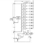
LM3914 block diagram.JPG

Definitely not aimed at you, quite the opposite.

- - - Updated - - -

Hi SparkyChem,

Just to clarify:

The supply voltage you will have available for the LM3914 (and any additional circuitry needed) is +5V DC or +-5V DC or what?

What will the circuit be powered by, a wall wart/plug in power supply or a battery?

The input signal range maximum value is +-6V DC or what maximum value can it reach? Is the input signal AC or DC?

Otherwise, this feels rather like being asked to build a house but without knowing how many m2 are available for the foundations :).

Thanks.
 

Hi,

@d123:
Definitely not aimed at you, quite the opposite.
I didn´t take it as offense. Nothing to worry about.

And I agree, that the bjt shouldn´t be the problem...

Klaus
 

Hi SparkyChem,

Just grabbed an hour or so to fiddle a bit further with the idea. I can't help but feel that my version is parts-heavy and could surely be reduced if considered from another viewpoint. Anyway, here's the same version with a 555 added for the flashing functionality. I'm thinking about how to deal with the LM3914, personally, I'd suggest choosing either an exclamation mark version or a bargraph flasher but not try to combine both after looking at the schematics in the LM3914 datasheet more carefully...

Please bear in mind, this is just a circuit suggestion... The reason for the 4069 (or you can use the 4049, they're the same thing, basically) inverter IC is because otherwise the circuit has the undesirable quality/penalty of using more current doing nothing than when there are overvoltage events due to how comparators work, so it seems wiser to have the comparator inputs as in the schematic and add the inverter IC to use less current overall, milliamps or not, with a battery it would be not good to squander current...

The schematic:

LM3914 rough idea schematic v2.JPG

The results of a simulation:

LM3914 rough idea v2 transient graph a.JPG

A close-up of what the 555 and NPN will do when the voltage is at or over (in this design) +6V or - 6V:

LM3914 rough idea v2 transient graph b 555 detail.JPG
 

Hi,

Did a couple of sums for the LM3914...if I've understood what the datasheet requires...

First set of calculations were for a 3V full scale, but that is hard, i.e. weird-looking, to divide 6V into 10 LEDs and 3mA per LED. Also calculated for around 9mA per LED.
You can have the results if that scale appeals to you.

To use 6 LEDs to represent 6V input for the Ref pin rigmarole and the internal divider scale I would suggest dividing each input Volt down to 500mV. Four LEDs would be unused on both LM3914s unless you want to do the flashing bargraph version.

R1 = 4.9K
R2 = 10K

I LED = 3mA.

Not willing to spend another hour doing yet more iterative calculations for about 10mA LED current, I'll leave that pleasure for you. 3mA should be more than bright enough for average LEDs.

Ref Vout = (1.25V * (1 + (10000/4900))) + (0.00012A * 10000)
Ref Vout = 5.001V
Therefore each LED will turn on at 500mV increments from 0V to 5V, which represents a real world scale of 0V to 10V.

I LED = (5.001V/14900 Ohms) * 10
I LED = 0.0033A

For the above scale all you need to do is divide the input voltage by 2. That could be accomplished by a voltage divider made up of two 5.1K resistors. The LM3914 signal input must be limited to below 3mA.

"INTERNAL VOLTAGE REFERENCE" and "CURRENT PROGRAMMING" descriptions are on page 9 of the datasheet.
"2) Pin 5 input current must be limited to ±3mA." Notes at the bottom of page 3 of the datasheet.

Using 6 LEDs in a straightforward way that is simple to interpret and lighting up all ten for the positive and negative overvoltage events seems okay to me. The exclamation mark version lights up the number of LEDs that correspond to the input voltage.

How have you been getting along with this circuit?
 

Hi SparkyChem,

You are still alive, and keen, are you? ;)

Without wanting to sound too stroppy:

What's the limit at both ends for the exclamation mark (or the bargraph) to flash, +-5V or +-6V? Big difference.

It's neither clear from your first post nor from post #10. You keep saying +-5V and +-6V in the same thread posts...

It's pretty pointless for me to try to calculate this circuit when that aspect isn't clear to me, I'm afraid. I'm also having to guess that the supply voltage is +5V DC. I'm not doing theoretical homework for fun, I'm using my free time to try to help you. Some clear input from yourself would be appreciated if you are still planning on making this circuit.

My conclusion so far to make this as simple as possible is to separate this off into two LM3914 exclamation mark circuits. One will display negative voltages and the exclamation mark at -5V (or -6V) while the other will have no LEDs lit up and vice versa for +5V (or +6V). Each will use up to six LEDs/outputs and the "dot" one that is not an output but only goes on when the limit voltage is reached to flash the "exclamation mark". The exclamation mark version lights up one LED per Volt input signal according to the description in the datasheet.

How much current do you want for the LEDs? 3mA is more than enough for hand-held devices or something in the same room as the viewer. If you plan to illuminate a football stadium and want to max. out the output current to ~20mA per LED (with all 10 LEDs on) then it would help to know :). The device can dissipate 1365mW. 10 * 25mA = 0.25A. 0.25A * 5V = 1.25W. Adding for housekeeping current the LM3914 will use, I'd guess the max. per LED is realistically about 20mA to 25mA, this amount of current is OTT for most LEDs and a waste of energy IMHO, and the LEDs will wear out sooner. Ant the LM3914 will get nice and hot, and wear out sooner. "Less is more" in the long run, I would say. Maybe 10mA if needs must, but as I said, 3mA to 5mA is ample LED current. Always derate and avoid several undesired issues.

Your explanatory diagram in post#10, translating +-6V signal to +-5V with 10 LEDs - as I said above somewhere - is pretty grim. Think about it, the numbers don't fit: 20 outputs and representing +-12V with them - that's not intuitive to the eye/brain. I'd want something that at a glance the lit-up LEDs told me the actual voltage, not making me do mental arithmetic. If I'm wrong about this assumption, let me know and my apologies.

The LM3914 datasheet points out the issue of:
"DOT OR BAR MODE SELECTION
The voltage at pin 9 is sensed by comparator C1, nominally referenced to (V+ − 100mV). The chip is in bar mode
when pin 9 is above this level; otherwise it's in dot mode. The comparator is designed so that pin 9 can be left
open circuit for dot mode.
Taking into account comparator gain and variation in the 100mV reference level, pin 9 should be no more than
20mV below V+ for bar mode
and more than 200mV below V+ (or open circuit) for dot mode. In most
applications, pin 9 is either open (dot mode) or tied to V+ (bar mode). In bar mode, pin 9 should be connected
directly to pin 3. Large currents drawn from the power supply (LED current, for example) should not share this
path so that large IR drops are avoided."

In my opinion, unless I'm missing something, a miserably tiny 20mV max from V+ makes trying to alternate between dot mode and bar mode unlikely with any blocking/pass device I can think of due to inevitable voltage drop across a BJT or a MOSFET or a relay or anything else on this planet I can think of as a pass device apart from thin air so as to alternate between the two modes... I strongly recommend selecting one circuit or another but not hoping to combine three different ones from the datasheet as though this were a pick-n-mix sweet shop.

I'm trying to help, even if it may not always sound like it.

- - - Updated - - -

...Whoops, extremely bad mental lapse there...

5V LED supply - 1.7V LED Vf = 3.3V into LM3914 "outputs".
3.3V * 0.025A LED current = 0.0825W.
0.0825W * 10 "outputs" on = 825mW.
Supposedly the LM3914 comsumes about 10mA or so = 50mW
Total PD at all LEDs on presumably around 0.9W...

I'd still avoid that level of power dissipation unless it's momentary and sporadic.
 

Hi,


Still there is some misunderstanding.

For sure you can't find the value for the load current in the bjt datasheet.
If the load is a standard LED fir example you may set the LED current to 20mA... then the LED is the load
The LED current = the load current = the collectir current.
For a motor it may be 2A, for a relay it may be 70mA .... it simply depends on the circuit connected to the collector

Klaus

Thanks for the clarification. I re-read the #2 post from where you used ohm's law. As mentioned I thought that this was not recommended to get an "exact result". But it looks that a raw estimation is okay for this application. Still, I am left pondering. Will it be proven using nodal analysis that those values are okay?. Although it is not specifically stated in the answer, 1.5 kOhm comes from dividing 3V/2mA. While it is mentioned that a more precise calculation would consider V_BE_ON to 0.6V is something which I intended to do with the calculations that follow but again this was not right. Therefore, If had desired to do that specific calculation, how would be done?. I mean using nodal analysis.

Yes I get what you meant with the load determines the current to be drawn by the transistor. I thought that in its max then I could use that value, which of course I wouldn't expect to go that far, anyway I think that for designing purposes I'd select the highest value.

Usually I thought that the way to go when calculating the adequate value for the resistor would require nodal analysis as it is something which I'm familiar from circuit analysis as it seems more logical as this includes transistor's gain and so on. Whereas dividing by 10 and the rest that you mentioned left me dumbfounded from where do those values comes from. Again, I didn't know that using ohm's law in such straight manner is allowed. I thought there was some justification of doing so. But if that's okay, i'll take it as the way to go.

There's a passage which I read from Malvino's Electronic principles which states like this:

The desired result depends on the level of accuracy you want to achieve. The finer to the nearest approximation, the result will be to the real value.

Therefore I thought that nodal analysis would explain what value to choose.

Just for clarification I'm "he"

Hi SparkyChem,

Just to clarify:

The supply voltage you will have available for the LM3914 (and any additional circuitry needed) is +5V DC or +-5V DC or what?

What will the circuit be powered by, a wall wart/plug in power supply or a battery?

The input signal range maximum value is +-6V DC or what maximum value can it reach? Is the input signal AC or DC?

Otherwise, this feels rather like being asked to build a house but without knowing how many m2 are available for the foundations :).

Thanks.

Answering your question the circuit will be powered by a 9V battery althought I could use a wall wart or plug, since higher voltage will be needed to fed LM3914 to register higher values in the input. As mentioned in the requirements +- 6VD will be the max signal as DC.


Hi SparkyChem,

Just grabbed an hour or so to fiddle a bit further with the idea. I can't help but feel that my version is parts-heavy and could surely be reduced if considered from another viewpoint. Anyway, here's the same version with a 555 added for the flashing functionality. I'm thinking about how to deal with the LM3914, personally, I'd suggest choosing either an exclamation mark version or a bargraph flasher but not try to combine both after looking at the schematics in the LM3914 datasheet more carefully...

Please bear in mind, this is just a circuit suggestion... The reason for the 4069 (or you can use the 4049, they're the same thing, basically) inverter IC is because otherwise the circuit has the undesirable quality/penalty of using more current doing nothing than when there are overvoltage events due to how comparators work, so it seems wiser to have the comparator inputs as in the schematic and add the inverter IC to use less current overall, milliamps or not, with a battery it would be not good to squander current...

The schematic:

View attachment 149821

The results of a simulation:

View attachment 149822

A close-up of what the 555 and NPN will do when the voltage is at or over (in this design) +6V or - 6V:

View attachment 149823

Thanks for taking time into looking at my problem. As you mentioned is a suggestion. Surely it has lots of parts and certainly it looks acceptable. But have you tested it?.

I don't know how it will behave with the LM3914. Since this is not included in the simulation. I'd like to know how would be the result?

Hi,

Did a couple of sums for the LM3914...if I've understood what the datasheet requires...

First set of calculations were for a 3V full scale, but that is hard, i.e. weird-looking, to divide 6V into 10 LEDs and 3mA per LED. Also calculated for around 9mA per LED.
You can have the results if that scale appeals to you.

To use 6 LEDs to represent 6V input for the Ref pin rigmarole and the internal divider scale I would suggest dividing each input Volt down to 500mV. Four LEDs would be unused on both LM3914s unless you want to do the flashing bargraph version.

R1 = 4.9K
R2 = 10K

I LED = 3mA.

Not willing to spend another hour doing yet more iterative calculations for about 10mA LED current, I'll leave that pleasure for you. 3mA should be more than bright enough for average LEDs.

Ref Vout = (1.25V * (1 + (10000/4900))) + (0.00012A * 10000)
Ref Vout = 5.001V
Therefore each LED will turn on at 500mV increments from 0V to 5V, which represents a real world scale of 0V to 10V.

I LED = (5.001V/14900 Ohms) * 10
I LED = 0.0033A

For the above scale all you need to do is divide the input voltage by 2. That could be accomplished by a voltage divider made up of two 5.1K resistors. The LM3914 signal input must be limited to below 3mA.

"INTERNAL VOLTAGE REFERENCE" and "CURRENT PROGRAMMING" descriptions are on page 9 of the datasheet.
"2) Pin 5 input current must be limited to ±3mA." Notes at the bottom of page 3 of the datasheet.

Using 6 LEDs in a straightforward way that is simple to interpret and lighting up all ten for the positive and negative overvoltage events seems okay to me. The exclamation mark version lights up the number of LEDs that correspond to the input voltage.

How have you been getting along with this circuit?

Thanks for letting me know the required calculations.

I'm still trying to understand the circuit, but the stage where I'm stuck at is where comparator inverter comes into place. This uses 555 for generating pulses. But this means that is the timer flashes the leds and not exactly a job that might be doing the LM3914 which it was the main premise of the question. However I'm okay with the omission of this just for the sake of getting the desired end result. Yet. I'm not sure if you tried, but can you please post a simulation of how will it work with the LM3914?


Hi SparkyChem,

You are still alive, and keen, are you? ;)

Without wanting to sound too stroppy:

What's the limit at both ends for the exclamation mark (or the bargraph) to flash, +-5V or +-6V? Big difference.

It's neither clear from your first post nor from post #10. You keep saying +-5V and +-6V in the same thread posts...

It's pretty pointless for me to try to calculate this circuit when that aspect isn't clear to me, I'm afraid. I'm also having to guess that the supply voltage is +5V DC. I'm not doing theoretical homework for fun, I'm using my free time to try to help you. Some clear input from yourself would be appreciated if you are still planning on making this circuit.

My conclusion so far to make this as simple as possible is to separate this off into two LM3914 exclamation mark circuits. One will display negative voltages and the exclamation mark at -5V (or -6V) while the other will have no LEDs lit up and vice versa for +5V (or +6V). Each will use up to six LEDs/outputs and the "dot" one that is not an output but only goes on when the limit voltage is reached to flash the "exclamation mark". The exclamation mark version lights up one LED per Volt input signal according to the description in the datasheet.

How much current do you want for the LEDs? 3mA is more than enough for hand-held devices or something in the same room as the viewer. If you plan to illuminate a football stadium and want to max. out the output current to ~20mA per LED (with all 10 LEDs on) then it would help to know :). The device can dissipate 1365mW. 10 * 25mA = 0.25A. 0.25A * 5V = 1.25W. Adding for housekeeping current the LM3914 will use, I'd guess the max. per LED is realistically about 20mA to 25mA, this amount of current is OTT for most LEDs and a waste of energy IMHO, and the LEDs will wear out sooner. Ant the LM3914 will get nice and hot, and wear out sooner. "Less is more" in the long run, I would say. Maybe 10mA if needs must, but as I said, 3mA to 5mA is ample LED current. Always derate and avoid several undesired issues.

Your explanatory diagram in post#10, translating +-6V signal to +-5V with 10 LEDs - as I said above somewhere - is pretty grim. Think about it, the numbers don't fit: 20 outputs and representing +-12V with them - that's not intuitive to the eye/brain. I'd want something that at a glance the lit-up LEDs told me the actual voltage, not making me do mental arithmetic. If I'm wrong about this assumption, let me know and my apologies.

The LM3914 datasheet points out the issue of:
"DOT OR BAR MODE SELECTION
The voltage at pin 9 is sensed by comparator C1, nominally referenced to (V+ − 100mV). The chip is in bar mode
when pin 9 is above this level; otherwise it's in dot mode. The comparator is designed so that pin 9 can be left
open circuit for dot mode.
Taking into account comparator gain and variation in the 100mV reference level, pin 9 should be no more than
20mV below V+ for bar mode
and more than 200mV below V+ (or open circuit) for dot mode. In most
applications, pin 9 is either open (dot mode) or tied to V+ (bar mode). In bar mode, pin 9 should be connected
directly to pin 3. Large currents drawn from the power supply (LED current, for example) should not share this
path so that large IR drops are avoided."

In my opinion, unless I'm missing something, a miserably tiny 20mV max from V+ makes trying to alternate between dot mode and bar mode unlikely with any blocking/pass device I can think of due to inevitable voltage drop across a BJT or a MOSFET or a relay or anything else on this planet I can think of as a pass device apart from thin air so as to alternate between the two modes... I strongly recommend selecting one circuit or another but not hoping to combine three different ones from the datasheet as though this were a pick-n-mix sweet shop.

I'm trying to help, even if it may not always sound like it.

- - - Updated - - -

...Whoops, extremely bad mental lapse there...

5V LED supply - 1.7V LED Vf = 3.3V into LM3914 "outputs".
3.3V * 0.025A LED current = 0.0825W.
0.0825W * 10 "outputs" on = 825mW.
Supposedly the LM3914 comsumes about 10mA or so = 50mW
Total PD at all LEDs on presumably around 0.9W...

I'd still avoid that level of power dissipation unless it's momentary and sporadic.

I am so sorry about the delay in my response. In fact I had been recovering in my health. Anyways I explained in my last reply my intention was to use LM3914 as an indicator for two intervals of voltage, since in every application note I found there was only an example of how to use it between positive voltages.

Most of the simulation if not everything I do it with Proteus (ISIS) the version which I use is Proteus 8, what I like about it is that it makes it possible to "interact" with a variable resistor, thus you can change the value by sliding it during simulation. The same can be done with Multisim which I used it before. I had been recommended PSpice from LT but it does not offer much options and is by no means as near of what either Proteus or Multisim can offer. I'm not familiar with Tina TI 9, not sure if you can simulate what I explained above (a variable resistor) or perhaps a thermistor, photodiode or an LDR being exposed to light. (Luckily none of these are requirements are needed in this problem).

Thanks for the clarification about the stage involving amps. As I mentioned I didn't realized that pull-up resistor were necessary for this application.

I don't know if it adds to an answer for this riddle, but I found this article about using the LM3914. The author explains in figure 20 how an over range alarm driver circuit can be interfaced with the driver, although by doing so it requires an external alarm unit which is triggered when the last LED is ON. Although this is not what I was looking for since my intention was to rely on the LM3914 built in capacity to blink in over range
mode.

To be honest I'm not very savvy with digital electronics yet (I'm relying in reviewing what I don't understand with Floyd's Digital Fundamentals) but from your reply it looks that CD4047 can be used but for "space" and perhaps functionality 555 would be better. I'd like to note that I wasn't aware about the behavior you mentioned on the reset pin which happens during the power-up or deactivation.

I'm glad that the diagram could had made myself better understood, but just hope didn't caused any further confusion. I'm sorry if this riddle may seem convoluted or as you mentioned sisyphean, but I think maybe there is a way to make it without combining two circuits?.

Although what you say may sound reasonable about redundancy on using an exclamation point plus flashing bar graph. My intention was to know if the IC mentioned can work with those modes regardless regardless of any consideration or limitations in the design. Something closer to a challenge to the capacity of what could be achieved with the LM3914.

Yet, I'd like to note again that a simulation of how would your circuit behave with LM3914 would be desired. I do not have the components at hand and I'd like to know if it gets any close with the result.
 

Status
Not open for further replies.

Part and Inventory Search

Welcome to EDABoard.com

Sponsor

Back
Top