Continue to Site

Welcome to EDAboard.com

Welcome to our site! EDAboard.com is an international Electronics Discussion Forum focused on EDA software, circuits, schematics, books, theory, papers, asic, pld, 8051, DSP, Network, RF, Analog Design, PCB, Service Manuals... and a whole lot more! To participate you need to register. Registration is free. Click here to register now.

H-bridge Mosfet protection

Status
Not open for further replies.

Em_13

Junior Member level 3
Joined
Feb 7, 2016
Messages
28
Helped
0
Reputation
0
Reaction score
0
Trophy points
1
Activity points
232
I have built a 220v pure sine inverter using EG8010 spwm ASIC.
the Circuit is overload protected by using shunt and op-amp,But It's not protected from output sparks.
Here is the original circuit:
EGS002_manual_en_2-page-001.jpg

Every thing is OK,Except when we have spark at output which leads one or more mosfet and even driver IC to burn.
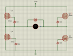
Can I put 13 or 15v zener diode between source and gates to protect mosfets and driver ICs like this:
45.PNG
 

Hi,

the MOSFET internal body diodes should caryy the current and thus limit the voltage.
But to do this, they need a low impedance path for current flow.

But in your schematic there is no capacitor from high_side_mosfet_drain to GND-plane.
You need to install a common electrolytic bulk capacitor. .. and individual (two pieces) foil capacitors with very short connection from Mosfet_drain to GND.

For sure this needs a good PCB layout with proper GND plane.
Then this should be sufficient to protet the MOSFETs from overvoltage fail.
No need for the zeners at the gates, then.

Klaus
 
  • Like
Reactions: Em_13

    Em_13

    Points: 2
    Helpful Answer Positive Rating
Thanks dear klaus for your reply,But I have used electrolyte cap(2*82uf) and two 100nf CBB cap very close to mosfets in my PCB.
Does placing the 16V zener diodes on mosfet's GS cause a problem?
 
Last edited:

,But It's not protected from output sparks.

Please elaborate: what is the exact source and nature of the output sparks?
 

Why did you place a reverse diode across the gate resistor will it not make your turn turn OFF very fast ? It will increase your dv/dt substantially and reduce the short circuit

withstanding capacity.
 

Hi,
@nikhilmahasvar
Why did you place a reverse diode across the gate resistor will it not make your turn turn OFF very fast ? It will increase your dv/dt substantially and reduce the short circuit

withstanding capacity.
This is the usual H-bridge circuit.
And yes: the job is to make turn OFF faster .. to avoid cross conducting of high side and low side Mosfets.
The circuit is correct in this.

Klaus
 

You are experiencing inverter damage in case of intentional output short. I presume you haven't been able to determine if it occurs due to delayed overcurrent shutdown and respective exceeding of MOSFET maximum ratings or malfunction caused by "sparks", e.g. voltage transient brought up by discharging the output filter capacitor.

I'm not even sure if the overload protection is guaranteed to handle shorts or only moderate output overload. I agree with others that gate-source zener diodes have probably no effect regarding the observed circuit damage.

Does your setup include the output filter shown in the "original circuit"?
 
  • Like
Reactions: Em_13

    Em_13

    Points: 2
    Helpful Answer Positive Rating
Does your setup include the output filter shown in the "original circuit"?
Yes,of course.Filter consists of 3.3uH + 2.2 uF as datasheet.

voltage transient brought up by discharging the output filter capacitor.
I think You are right.So I placed bidirectional 350V TVS at h-bridge output and maybe it suppress TV and solve problem but I don't test it in practice.


You mentioned that gate zener diode maybe useless.I have no experience in this type of circuits,Please tell me that does placing zener diode for high side mosfets't gate cause a problem?
 
Last edited:

The circuit diagram looks fine (I cannot find any fault but...) - what about stray capacitance and inductance? The driver ICs and the mosfets - are they connected by long wires? The spark at the output produces oscillations and the resonant voltages are not been able to be suppressed by the diodes- perhaps they are too fast. It is a random guess: try changing the value of L1 such that L1C2 resonance is shifted to a much lower frequency.
 

Please tell me that does placing zener diode for high side mosfets't gate cause a problem?
I don't think so.
Filter consists of 3.3uH + 2.2 uF as datasheet.
Results in about 60 kHz cut-off frequency, makes no sense. 3.3 uH means that output shorts cause very fast MOSFET current rise, little chance for overcurrent protections to act before the transistors are damaged.

- - - Updated - - -

EG8010 datasheet suggests, 3.3 mH inductor. What's the actual inductance value and inductor type?
 
  • Like
Reactions: Em_13

    Em_13

    Points: 2
    Helpful Answer Positive Rating
Sorry for misspelling.I made 3.3mH with 33*29 EI ferrite.
How about this circuit that uses an odd and of course interesting method to protect driver ic?
After mosfets burn,mostly All three legs of mosfet will short circuit to each other.therefor it cause damage to driver.
This circuit employ fuse and zener(Maybe it could be called FD circuit!) to protect LO and HO pin of driver.

ssssssssss.PNG
 
Last edited:

I made 3.3mH with 33*29 EI ferrite.
The small core suggests an inductor without air gap, saturated at higher output current and thus not limiting di/dt during short circuit.

This circuit employ fuse and zener(Maybe it could be called FD circuit!) to protect LO and HO pin of driver.
Fuse is far too slow to protect gate driver.
 

What is the designed output power level (at the input and also at the output)? The inductor at the output is apparently not doing its job.

Is it possible to reduce the capacitor value at the output? - just a wild guess!!
 

Fuse is far too slow to protect gate driver.
Actually fuse does not protect mosfet.
It is to protect driver,In the presence of a zener or TVS diode,It just disconnect HO or LO from Gate after mosfet burns(As I said above three legs of mosfet is directly connects together in case of mosfet burns.for example 325v directly conducted to HO or LO and destroy internal output transistor for a split second)
zener or TVS diode protects both.


What is the designed output power level (at the input and also at the output)? The inductor at the output is apparently not doing its job.
Is it possible to reduce the capacitor value at the output? - just a wild guess!!

My push-pull circuit(DC-DC , 12V to 325V)has more than 500W power but in DC-AC stage using 4*IRF840 limit the power to about 300 or 400W.
Inductor and capacitor value is based on datasheet and ready modules on the market.


I placed TVS+zener diode between SD AND SG of mosfets.I want to use 100mA fuse instead of 400mA.But i don't have them right now to test circuit against Intentional short circuit.I will test is as soon as I got them.
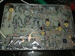
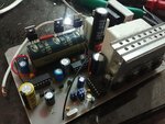
Here is my circuit:

photo_2018-10-28_20-18-43.jpgphoto_2018-10-28_20-18-29.jpg
 

Hi,

I see your PCB. It has no GND plane, thus you will have a lot of stray inductanct. This makes it very difficult to keep voltage peaks low.
I see those voktage peaks as the main problem that kill your Mosfets.

I strongly recommend to design a new PCB with proper, solid GND plane.

Klaus
 
  • Like
Reactions: Em_13

    Em_13

    Points: 2
    Helpful Answer Positive Rating
I see those voktage peaks as the main problem that kill your Mosfets..

Right and they are now unpredictable.

Slow down, if possible. But if you must, you need soft turn on and turn off. Also increase the dead time. Perhaps it may work ...
 
  • Like
Reactions: Em_13

    Em_13

    Points: 2
    Helpful Answer Positive Rating
Status
Not open for further replies.

Similar threads

Part and Inventory Search

Welcome to EDABoard.com

Sponsor

Back
Top