Continue to Site

Welcome to EDAboard.com

Welcome to our site! EDAboard.com is an international Electronics Discussion Forum focused on EDA software, circuits, schematics, books, theory, papers, asic, pld, 8051, DSP, Network, RF, Analog Design, PCB, Service Manuals... and a whole lot more! To participate you need to register. Registration is free. Click here to register now.

Need help stabilizing a switching regulator

Status
Not open for further replies.

Plecto

Full Member level 5
Joined
Jan 4, 2012
Messages
315
Helped
1
Reputation
2
Reaction score
1
Trophy points
1,298
Activity points
4,979
Hi. I need to design a switching regulator with 48V input, 0-40V, 0-10A output. I've chosen the LM5117 for this purpose. I want a pose a general question regarding switch mode regulators like these. If we disregard efficiency, component size and cost, and bandwidth, what would I do to make this regulator stable regardless of output voltage and output current? The output voltage is adjusted by a filtered PWM connected to the feedback path by the way.
 

Hi,

The datasheet tells you all you need to know.
If the circuit is not stable then most likely you didn't follow all datasheet recommendations.

Maybe you can find additional information in application notes.
Check the manufacturer's internet pages.

Klaus
 

Its just a case of making out the expression for the feedback loop……this means multiplying the power stage transfer function of your Buck, by the modulator transfer function, and by the error amplifier transfer function.
The “modulator transfer function” means the bit inside the LM5117.
When you have done the said multiplication, you have the open loop feedback loop transfer function expression………..and of course we are dealing with complex numbers here…so you are going to get plots of Gain vs frequency, and phase vs frequency……….so you need complex numbers because at each frequency, you don’t just have a loop gain, you have a loop phase aswell.
So make out your plots of the open loop transfer function as described….then you can read off your gain and phase margin. From that you get your stability
Remember to adjust the expression for whether you are in CCM or DCM.
Do this for each vout and Power out value.
If the datasheet doesn’t help, then Bassos books help out with the transfer functions that you need.
Remember your phase should best be more than 45 degrees at the crossover point…..and a decade in frequency beyond your crossover point, the gain should have dropped lower than -10dB.
The crossover point is where your loop gain goes down to zero dB.
So yes its best to work in dB…then you just add stuff instead of multiplying.
Remember that when converting to dB…….Gain in dB = 20 x (log_to_the_base_10) [Vout / Vin].
The vout/vin is what you get out of Bassos equations….there will obviously be a value for each frequency, so sweep the frequency , and calculate for each frequency, doing it in excel or Mathcad helps.
You get a chart like in the attached.
 

Attachments

  • Feedback loop calculation example.zip
    2.8 MB · Views: 90

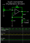
The buck converter can be regulated in a straightforward manner, by switching it On and Off as output voltage varies above and below a chosen threshold.

This simulated buck converter is based around an op amp which is an ideal model unlike real op amps. Its output voltage is the same as your spec 48 V.

On-off action is configured for hysteresis around the voltage selected by the potentiometer at left.
It has snap action due to its high gain.

op amp is buck conv 48V supply -load gets 20V 10A.png
 

Thanks for the replies. I've read the datasheet of the regulator, but there are a lot of confusion about loop compensation, 'adding dominant pole' and such terminology, I should really like a class in feedback circuit stability. I've also tried following the datasheet examples to the letter which leads to a stable regulator regardless of output voltage as long as the input voltage is kept below 20V or so, having 48V input causes instabilities at certain output voltages. Many of the formulas in the datasheet requires desired output voltage though, so I can't really follow the examples completely. The instability is in such a way that it draws loads of current (can't imagine anything else than shoot-through). As this is a work related project, there is a limit to how much time I can put into getting a complete understanding of how to stabilize a feedback loop like this, so I'm really just asking for a way to 'make sure' it's stable, I was thinking that this would be possible by having a really low bandwidth? Looking at the datasheet: https://www.ti.com/lit/ds/symlink/lm5117.pdf The components that I struggle understanding the purpose of are the COMP cap and resistor, as well as the RAMP cap and resistor. I'm also not sure if a snubber circuit is needed, or what is would have to say about these instability problems. I believe the board layout is alright though, components are very close together and all ground paths leads directly to a complete ground plane on the layer below.
 

The “RAMP”…..
All that is doing is emulating the ramp that you would see on a sense resistor if it were placed in the hi side , in series with the hi fet. That is, I mean the ramp of the inductor current as the fet is turned on
If you don’t understand this ill send you a sim.
If you look where the sense resistor is in the LM5117, its in the “wrong” place….it senses the off state current, rather than the on state current….so you need the RAMP to give you the on state current ramp…..i hope I explained it…if not, ill send you the sim I spoke of.
As the datasheet says, when you have very small duty cycles , (because vout/vin is very low), then the on state ramp would be “destroyed” by the turn on spike through the fet…..so what they have done is clever…they are not sensing the actual inductor current at turn on…instead, they are emulating what it would be like (but without the nasty turn on spike)….the RAMP cap Is supposed to emulate what the ramp would be like in an ideal situation with a hi side sense resistor.
Another reason for emulated current mode is because at small duty cycles, the gate turn on current can “destroy” the sensed inductor ramp signal in the sense resistor……..if the duty cycle is longer then you can use “leading edge blanking time” to ignore the sense signal just after fet turn on…..but you cant do that with low duty cycles, because the on time is less than the LEB time.
Other advantages are that since your current sense is in the low side. You don’t need the extra circuitry to read its voltage.
I realise I haven’t explained well, but the datasheet, explains it poorly IMHO.
The COMP cap forms part of the error amplifier transfer function……..can you produce the transfer function for the error amplifier?....i haven’t fully read lm5117 datasheet, but error amplifiers are usually opamp integrators…….so you usually work it out by the transfer function for that opamp….but maybe the lm5117 uses a transconductance amp , I don’t know………they should give you the transfer fucntions I spoke about, then you wade through the math and get the open loop transfer function, then you can asses the stability………and yes, generally speaking, the lower your bandwidth, (crossover frequency) then usually the easier it is to stabilise the feedback loop.
 

Status
Not open for further replies.

Similar threads

Part and Inventory Search

Welcome to EDABoard.com

Sponsor

Back
Top