Continue to Site

Welcome to EDAboard.com

Welcome to our site! EDAboard.com is an international Electronics Discussion Forum focused on EDA software, circuits, schematics, books, theory, papers, asic, pld, 8051, DSP, Network, RF, Analog Design, PCB, Service Manuals... and a whole lot more! To participate you need to register. Registration is free. Click here to register now.

Help re-creating a replica movie prop

Status
Not open for further replies.
No offense taken! The manner in which I'm doing things just shows my inexperience, haha. Thankfully, I'm on the home stretch and once the 555 circuit is corrected, the board is finished. Then I can spend a month populating it with components and move into case fabrication. Still, its been super educational for me to do all this longhand (and I wasn't frustrated with the process at all). It's been really fun. I enjoy designing the circuits. Yes, thankfully, I'm using templates for major components. Vias for resistors are done manually so I can tighten up the spacing where needed.

So far, everything is made in ExpressPCB, and the test board I had made last month looks great. I design it, submit it, they fabricate and ship. I will add the contact points for the speaker. For the speaker: one lead goes to capacitor from pin 3 of second 555, the other goes to ground?

So, a second resistor is added BEFORE the capacitor coming from the diodes? Leave the existing resistor (before pin 2 of the 555) in place?

Can you recommend a way to replace the central trace with something better for the switches? I was thinking of just running them all independently to a new central point: a large pad, then going from the pad to pin 2 with the resistors/capacitor. Is that better?

Thanks again everyone,
John
 
Last edited:
Hi,

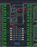
The added red bits are there to answer the speaker and 555 resistor questions. Both answers in words are yes and yes.

John movie prop replica PCB.JPG

I think there's nothing wrong nor worth changing about how you have done the central trace connecting the diodes to the resistor and capacitor junction nor the individual toggle switch connections to the diodes.

If it isn't a lifetime to incorporate, a solid ground plane is a wonderful thing to have.

SIL headers (male and female parts) are easy to snap off into 1's, 2's, 3's, etc. and save de-soldering and re-soldering if/when something goes wrong or you want to re-purpose an old part for something else. Can be a touch wobbly/loose, that's all. A dot of glue can ensure things stay in place. DIL headers are equally useful but a bit of a pita to break or cut apart, although a cutter/exacto knife is a good choice.
 
Thanks for the red markings, D. That is super helpful.
 

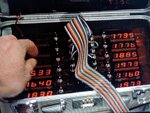
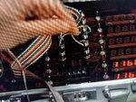
Took some snaps of the film tonight. You can see all the ICs all along the inside column between the two rows of digits. Somehow, they were able to group all 4 ics along the inside of each row of digits. As proud as I am, I had to scatter the 4 ICs per 4 digit number all around the row due to space constraints.

I keep trying, but I can't replicate the exact circuit layout in the film.

Take a look at the pics, lots of wires running from those toggles. Also note the single IC in the center, probably a 556.

Maybe they didn't use a circuit at all and it's all handwired, and that's how they were able to group the ICs so close.

MVIMG_20181219_000842.jpg

MVIMG_20181219_000640.jpg
 

Hi,

I doubt you can use only one diode, not sure to be honest. Test it on a breadboard.

I would think it were the other way around, the ICs are so close together because it's a PCB (maybe a multi-layer one) that doesn't have a kilo's worth and a cubic metre of cables underneath it.
 
Hard to see in pics, but if you look at the right edge of the board in the first photos, you can see lots of wires peeking out from beneath. Who knows how it was done!
 

It also looks like the displays are one module of four digits rather than four individual ones. You can't do it with one diode I'm afraid, they are there to isolate the switches from each other while still allowing any of them to make the beep. If you used one diode you would be linking all the toggles together which would stop the digit groups being latched as well.

Brian.
 

Hi Brian,

No worries on the Diodes, just asking. It's muddled in my phone pics of my TV screen, but on the Blu Ray you can see the individual digits grouped into 4s.

A side note: most, if not everything in the original prop seems to be Archer/Radio Shack, which makes sense for 1988. There are some other electronics props in the film with Motorola and RCA ICs as well.

I was able to identify a lot, and even get a lot of original vintage pieces, like the Digitran 23000 Thumbwheel, and vintage Archer alligator clips for instance, to make my replica as accurate as possible. I even found vintage-style, bevel-cornered digits made by Stanley. I couldn't find 48 vintage Archer digits!
 
Last edited:

I've read that traces can be very close together on low-powered circuits such as mine. If you guys can advise that the traces in the attached image look ok, then I've solved the grouping of the components. Attached is the left side of the briefcase, and as you can see, I was able to group the 4511s in 4 to the left of the 4 digits, exactly like the movie prop. This took a lot of thought, and some clever splitting of traces on the top and bottom layers of the board (green is bottom), without the use of vias! Not added yet are power and ground traces.

Thanks!
John

new.png
 

Traces down to 0.2mm are fine but check with the PCB manufacturer because it really comes down to how accurate their production processes are. You are missing the VSS and VDD power traces on the layout, I would suggest you add them and if possible make the traces as fat as possible, they carry most current and are most susceptible to noise so keeping as much copper in their connections will help. Note that it has nothing to do with the 'fuse' rating of the traces, it's just that the thinner they are the higher their resistance will be and higher resistance means more voltage drop per mA of current.

If you are going to hand wire to the tracks on the left side, fan the connection out and add pads to them so it's easier to attach the wires. Also remember that if you are going to replicate several of these designs to one sheet of PCB, they share a common supply and ground so you can link them with traces on the PCB. The less hand wiring the better!

Brian.
 
Hi Brian, thanks for all that! It prob got lost in my previous post, but I intentionally hadn't added power or ground traces before I knew it was worth my time to keep going with this. And yes, I will be fanning those traces on the left out to the pads (like my previous design).

Somehow, this new design has traces for everything, whereas the previous one required hand wiring in some places!

Oh, the diodes arrived yesterday. They're so tiny!

Thanks again,
John
 

You think those diodes are small..... I've got a 2.5"x2.5" bag here with 10,000 capacitors in it!

Tip: especially for the ground track, make it as fat as possible. Most designers would use 'flood fill' but it won't work with manual routing. Basically, it fills all the joinable voids on the board with copper to minimize the track resistance. It also helps in manufacture because boards start with a full copper layer and the gaps between tracks is chemically removed, if the gaps are filled in it means less copper has to be dissolved.

Brian.
 
How do you even handle a component that small?! I made the ground traces as beefy as possible, but I don't think this new design is going to work due to size constraints. I just need another inch or so. I'm so close, but I'm starting to think the actual prop used lots of jumpers to keep space down.

But, since I've gotten pretty good at designing circuits, I just don't want to revert to jumpers everywhere. I don't know.

I did find push-on female-to-female jumpers, but I'm not sure if they're small enough to grip those tiny IC and 7 Segment pins.

If they are, I can greatly reduce the amount of traces and overall size by using push-on jumpers in many places. Though they might wiggle free over time, requiring me to open the guts and resecure connections.

Your thoughts?
 
Last edited:

General rule: never clip anything to a component leg, it WILL fall off sooner or later!

Sometimes there is no option but to add a wire jumper, do your best to add a pad where a wire will have to go though so at least it doesn't strain any component when you solder it. If the only option is to add a wire, at least make it as easy as possible to do so.

Brian.
 
Hi,

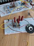
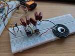
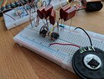
I'm very confused with the 555. I populated a breadboard, using my circuit and D's schematic for component placement. I don't have the 82k resistors, so I used 47ks.

I'm getting a cracking click from the speaker, and at times it seems to be dimming some of the digits and fouling up the segments. Any thoughts?

MVIMG_20181223_134535.jpgMVIMG_20181223_134540.jpg
 
Last edited:

It should work with 47K resistors but the tone or period may be wrong, they are OK to see if it works though.

I suspect the problem is you do not have a resistor in series with the loudspeaker. It is marked 8 Ohms which means it will have a DC resistance a little lower than that. The result is that when the output of the second 555 goes high, it will try to put full supply voltage across the loudspeaker and far too much current will flow. For a 9V supply which I think is what you are using, it will try to push more than an Amp through the speaker coil. That's enough that the 555 doesn't stand a chance of working and it will probably also pull the supply voltage right down (hence the dimming). You should add a resistor to limit the current, I would suggest no lower then 100 Ohms to keep things within specification.

It's difficult to see but I think you also have the diode reversed, it won't do any harm but it will stop the trigger operating.

Brian.
 
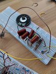
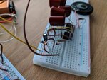
I definitely had a few wires crossed that I've since fixed. I took more photos that hopefully help. I always had a resistor on pin 3 to speaker, but maybe I have it wrong.

Do those red capacitors have a certain way of going to ground? I don't see markings. The smaller black Capacitor has clear markings I followed. I have the diodes negative facing away from the power bus. Is that right?

MVIMG_20181223_143756.jpgMVIMG_20181223_143801.jpgMVIMG_20181223_143818.jpg
 

Still looks wrong to me. On that kind of prototyping board, all the rows from the center to the outside are linked together except the outermost blue and red ones. For example A,B,C,D and E are linked together on each row. It looks like the resistor in series with the loudspeaker is therefor shorted out as is the diode at the input. You need to fit the components so each end is on a different row.

Those brown capacitors are not polarized so no worries about which way you fit them.

Brian.
 
Ah! I think I'm following, but not entirely sure. Also, shorted out as in grab new ones, these are fried??
 

Status
Not open for further replies.

Part and Inventory Search

Welcome to EDABoard.com

Sponsor

Back
Top