Continue to Site

Welcome to EDAboard.com

Welcome to our site! EDAboard.com is an international Electronics Discussion Forum focused on EDA software, circuits, schematics, books, theory, papers, asic, pld, 8051, DSP, Network, RF, Analog Design, PCB, Service Manuals... and a whole lot more! To participate you need to register. Registration is free. Click here to register now.

Help re-creating a replica movie prop

Status
Not open for further replies.
I have Express PCB. It's easier for me to do preliminary sketches in Illustrator. I will recreate it in Express PCB today.

As for the other 8 pins of the 4511s, they will be connected by wire from beneath the board, no traces, to save space in the case. I think this is going to work. If it doesn't, the entire case has to be hand wired.

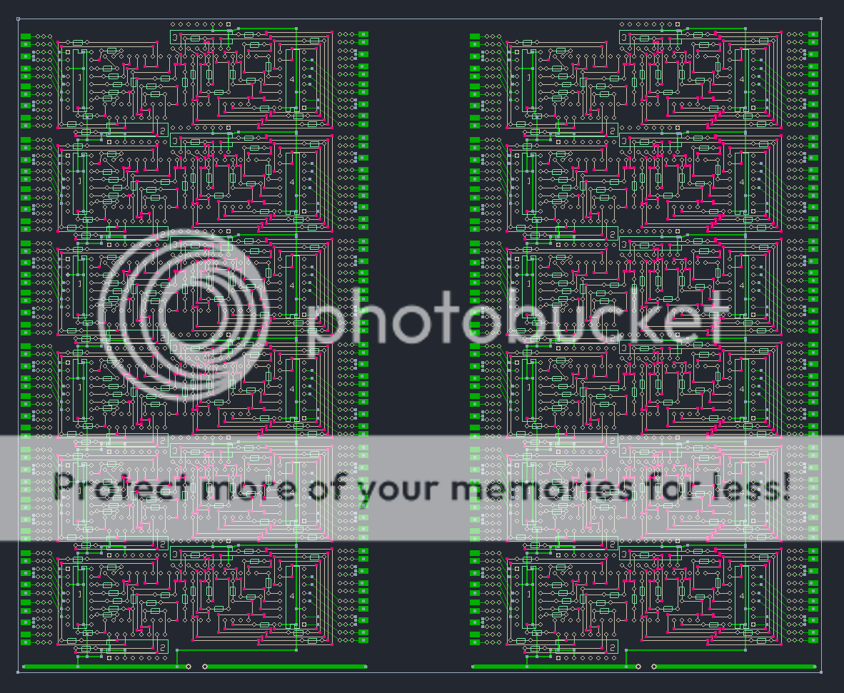
I've since created the right side circuit, too!

I'm also wondering I could use the chemicals and make my own board. I do have a Dremel press, but still, it's a lot of holes to drill!!
 

You can make your own boards and there are several ways to do it. I would advise against the "toner transfer" method as it tends to give unpredictable results and the design print can only be used once. A far better way is to print the artwork on transparent film (like overhead projector film) then use it several times to make identical PCBs. You need a UV exposure box which can be built relatively cheaply and either prepared photo sensitive PCB or plain PCB and spray it with photo sensitive paint. You expose the PCB to the UV light through the film in the same way as a photographic contact print is made. After a few seconds of exposure you chemically remove the unwanted resist paint so the copper you want to remove is exposed then dunk it in ferric chloride solution to remove the unwanted copper.
There is a short article here about it: http://www.atv-projects.com/Making_PCBs.html

Another way is isolation routing where you use an X-Y plotter or a 3D printer with a spinning cutter instead of the pen. The artwork has to be prepared specially for this process because it can only remove a thin sliver of copper at a time and may have to go back and forth many times to clear a big area. The principle is simple - start with a copper plated board and cut away the bits you don't want. There are lots of videos on Youtube about this method, it is slow but accurate and doesn't require any chemicals at all but the initial cost of machinery is higher.

Brian.
 

If I opt for two sided printing from a manufacturer, th n j csntrchnicall add the traces for rest of the 4511 chips on the under side and forego jumper wires, right?

Is that how two sided works? Additional traces for complex circuits like mine?
 

That looks a bit garbled but yes, the idea of double sided and indeed multi-layer boards is you can add more crossing wires without them contacting each other. With a little care you should be able to design the 4511 and associated components on to one board. I'm not sure of the final dimensions you have to work within but you might for example be able to fit several rows of 4 digits along with the drivers on to one board.

Brian.
 

Big step forward!

I moved into Express PCB using my Illustrator file as reference when it dawned on me that if I rotated some of the 4511s vertically, I would reduce the bulkiness of the circuit. About halfway through drawing this one I printed to check against my components, and everything fit beautifully! I'm really excited to have these made.

**broken link removed**
 

Well done.
Suggestions, and I'm aware that you are climbing a learning curve at your own speed so please take this as constructive, not critical:

1. By the time the holes have been drilled there will barely be enough copper around them to solder to. See it you can use larger pads.
2. You haven't allowed anywhere to connect wires to. If a connection is needed 'off board' add a pad for soldering the wire (or fitting a socket).
3. The ground and supply connections to the ICs are missing.
4. All the resistors are missing.

If space is a constraint, you could consider splitting the design differently, putting only the displays on one board and the remainder on a second board mounted elsewhere. If you do that, remember you still need somewhere to solder the wires to and you also need some method the mount the board to the front panel.

Brian.
 

Was up until 4am. I worked on it so much that I was able to really simplify (more so than my previous post) and make it symmetrical. Now it's only one circuit design that works on both the left and right side.

This will be a two sided board. Top side (which I just completed) only carries current from 4511s to 7 Segments, including their resistors (which I added this last round). Top has 1,920 holes in total!

The bottom side will carry power/ground as well as input (and resistors) from Thumbwheel to 4511s.

Most importantly, the space between the rows of digits and how the entire board fits in the briefcase matches the movie prop perfectly! This should turn out 100% accurate!

Need a break before sketching the bottom side traces.
 

I'm reading Mim's Engineer's Notebook, it's a great vintage resource for novices. Seems like I can make the chirp with a 3909 instead of a 555. The schematic is very simple, too. I can also connect a 5mm LED to flash.
 

I'm reading Mim's Engineer's Notebook, it's a great vintage resource for novices. Seems like I can make the chirp with a 3909

Mine is an original copy (1979) and I still keep it where I can quickly open it up.

The 3909 IC is no longer easily available. It was convenient to provide 2-3 volt flashes (or clicks) from a 1.5V battery.

The 555 IC is cheap and easy to work with.
There are many ways to make chirp circuits. The oscillator can be made from two invert-gates, resistor and capacitor.
The power source can be a capacitor with a value which discharges in 1/10 second. Charge it through a resistor chosen to do so in a few seconds.
 
I switched gears, now reading Mim's Getting Started with Electronics. This is a complete overview of electricity and circuits, great for me!
 

Agreed. Sadly you will find many of the classic components are no longer made and where stocks exist they are from 'buy up surplus' companies that charge the Earth.
The LM3909 went out of production about 30 years ago but it wouldn't be ideal in your situation anyway because it has a start up time before the first burst then bursts repetitively.

Unfortunately, many of the older devices you find on sales sites are fakes and simply don't work so avoid them if you can. I've just lost two days tracing an elusive software bug that was actually caused a fake MAX3232 IC. The purchaser eventually confessed they bought a batch on Ebay! Not one of the batch worked properly but a genuine one was fine. Lesson learned.

LM3909s were really designed as 1.5V powered LED flashers, bear in mind that an LED needs at least 1.6V before it lights up so you can see why they were useful. I use a discrete component version of one here as a marker beacon at the entrance to my house. It is absolutely dark here at night and finding that bottom step before I built the beacon resulted in lots of stubbed toes!

Brian.
 
Well, I never thought this day would come. I've created my first circuit, ever! It's two sided, and I just ordered a test board from ExpressPCB. If it works, I will duplicate and create either one larger 12 circuit board, or two smaller 6 circuit boards for the briefcase. As you can see, I really got the circuit down to a small size, and when ganged up in two rows of six (one over the other), the spacing and fit in the case matches the film prop perfectly, without an inch to spare. Due to size constraints, two digits have tracers, and two require jumpers, which I'm up for soldering.

Here's a pic
circuit-final.jpg
 
Last edited:

Major update. The test PCB (4-Digit) should arrive this Tuesday, Dec 4. Attached is the full, 12-Digit board, two rows of 6, with a spacious channel down the center. This matches the screen-used prop perfectly, and fits (now with room to spare) in the briefcase. I've spent a lot of hours refining this, and brought it to the most logical, user-friendly state I could given my size restrictions. I was able to add power traces to all 4511s, so that's 96 less pins that need to be jumped. I beefed up those traces to .20" Actually, now only two of the four 4511s (per readout) require jump wires, and only half of the pins on those chips. So, I greatly reduced the amount of wires I need to add.

I'd like to use that spacious channel down the center for the 555 (or 556) chips, with a speaker beneath the board in the bottom of the briefcase.

Brian,

I looked over your schematic, and for the most part I can follow it. I do see some new symbols (new to me), and have some questions. Are Uf and Nf Capacitors? This would be my first time working with them. Also, do they go to ground at all? Sorry, I'm sure your schematic explains everything to trained eyes, but I'm still figuring things out. I might have questions for you as I design the circuit for the 555 (or 556), so thanks in advance!

For instance, can I follow your schematic but swap the (2) 555s for a (1) 556, or does a new schematic have to be drawn? Can all 555/556 chips output to one speaker since they will beep at different times, and only once?

Anyway, here is the full circuit of 12 readouts, 6 per side.

 
Last edited:

Hi,

Nice modernist dayglo noodle maze there in your last post. You've put a lot of hard work into this circuit, good for you!

Are Uf and Nf Capacitors? This would be my first time working with them. Also, do they go to ground at all? Sorry, I'm sure your schematic explains everything to trained eyes, but I'm still figuring things out. I might have questions for you as I design the circuit for the 555 (or 556), so thanks in advance!

For instance, can I follow your schematic but swap the (2) 555s for a (1) 556, or does a new schematic have to be drawn? Can all 555/556 chips output to one speaker since they will beep at different times, and only once?


pF = picoFarads, e.g. 100pF = 0.000000000100 Farads
nF = nanoFarads, e.g. 100nF = 0.000000100 Farads
uF = microFarads, e.g. 100uF = 0.000100 Farads
mF = milliFarads, e.g. 100mF = 0.100 Farads
F = Farads, e.g. 1F = 1.000000000000 Farads ;)
milliFarads sounds to me like something from the time of Roswell and William Shockley, and women who worked in watch/telephone factories painting their teeth or parts of their houses with Radium for fun (true); more normal to say 1000uF. Most of life revolves around 10nF, 100nF, 1uF, 10uF, 100uF, to generalise enormously. When in doubt, count the E-n zeroes then add the number you need.

Yes, they do go to ground/0V in that schematic (but not always, depends on what you're doing, and using).

You can swap two 555s for one 556, the only things that need to be modified are the IC pin numbers, obtained by comparing and contrasting 555 and 556 datasheets.

I don't understand the last question, I think. If I have understood it, you would only need one 556 and one speaker and 12 diodes for the inputs. In the schematic Brian posted your inputs on the other end of the switches are ground.

I simulated this with 555s as the 556 in the simulator looks like a 555...

timer beep alternative schematic and transient results.JPG
 

In the schematic Brian posted your inputs on the other end of the switches are ground.
Sorry for not being so active on this topic. Yes, you only need one circuit triggered by closing any of the switches.
d123, as you have the simulation, can you show it over a longer time scale please, say up to 1 second to see that the beep (bottom waveform) stops after a few hundred mS.
It should beep once then stop if any of the switches are closed. These are the same switches that operate the row of digits.

Brian.
 

Hi guys,

Thanks for sharing the 555 schematic. Unfortunately, it’s just too confusing for my limited knowledge. I don’t think I’m capable of creating a circuit for it.

I linked a video below. The circuit in it uses less components and appears to do what I want. It was taken directly from Forrest Mimm’s book on 555 circuits. It’s not me in the video. Couldn’t this work if I replace the LED with a speaker and wire 12 switches to pin 2?

https://youtu.be/Izs-1z-LekE
 
Last edited:

Hi Brian,

as you have the simulation, can you show it over a longer time scale please, say up to 1 second to see that the beep (bottom waveform) stops after a few hundred mS.
It should beep once then stop if any of the switches are closed. These are the same switches that operate the row of digits.

I just tried but the simulator is having a bad maths day... It does "convergence issue" no matter how I set it to parse the circuit, and guess what? - It hits "convergence issue" whenever the astable timer should go low :). One thing is that the monostable will never go low as long as any switch is at ground potential, unless trigger is ac coupled; that may be the problem for the simulator.

As I can't make the switches work during transient simulations, not much more I can do, except for replacing a switch with a squarewave voltage source...

- - - Updated - - -

Hi,

1) Thanks for sharing the 555 schematic. Unfortunately, it’s just too confusing for my limited knowledge. I don’t think I’m capable of creating a circuit for it.

2) I linked a video below. The circuit in it uses less components and appears to do what I want. It was taken directly from Forrest Mimm’s book on 555 circuits. It’s not me in the video. Couldn’t this work if I replace the LED with a speaker and wire 12 switches to pin 2?

1) I'm confident of your ability to make that circuit work, anyway, a monostable is just as good.

2) Presumably yes, however we're back at the above observation: pin 2, "trigger" needs to be LOW for less time than the output pulse or the output will stay high as long as "trigger" is low. One could think of the 555 as just being two comparators with an internal reference voltage and that control the output being high or low. There is a solution to leaving "trigger" low longer than the output pulse duration...

555 trigger requirements 1.JPG

555 trigger requirements 2.JPG
 

I was assuming the switches were biased toggles so they would open themselves when released but adding the additional resistor and capacitor would fix the 'pulse' requirement for any type of switch. Only one resistor and cap are needed, the diodes still provide isolated paths to the switches on individual displays.

Brian.
 

Hi,

I've put together the 556 version for you, with a real 556. I don't have 82k or 6k8 resistors so I used 100k and 4k99 in their place instead, trivial and irrelevant difference.

Hate to repeat myself, but still - since the simulator doesn't have a 556 package, there are two TLC555s in the schematic, in the version on the breadboard I used an NE556N. Note that in the schematic the second timer (the one to the right) has "n/a" on its V+ and GND pins, that's because the 556 does not have two V+ and two GND pins, only pin 14 (V+) and pin 7 (GND).

There are only eight diodes and three "toggle" (A.K.A. "rocker") switches (one of the two switches is a two-way one) on the breadboard, which should be more than enough to show it works.

556 beep schematic working version.JPG

A (blurry) example of the circuit working. As you'll see in the video, it beeps at power-up - adding R1 and C1 stops that happening. C2 is needed, otherwise the 32 Ohm speaker I used was almost inaudible, 22uF to 100uF will make it even louder.

556 timer beep circuit video

Have fun!
 

I appreciate the effort here, gents. Thank you. But, I'm going with the YouTube video I posted last night--it's just easier for me. Even with your video, I don't know how to even start this circuit.

A couple of questions:
How can I add the 12 toggles to the YouTube circuit?
What would I need to adjust pitch and duration? Just different values of capacitors and resistors? I need a higher pitched tone and shorter duration than what was in your video, D123.

Thanks again!
John
 

Status
Not open for further replies.

Part and Inventory Search

Welcome to EDABoard.com

Sponsor

Back
Top