Continue to Site

Welcome to EDAboard.com

Welcome to our site! EDAboard.com is an international Electronics Discussion Forum focused on EDA software, circuits, schematics, books, theory, papers, asic, pld, 8051, DSP, Network, RF, Analog Design, PCB, Service Manuals... and a whole lot more! To participate you need to register. Registration is free. Click here to register now.

[SOLVED] High side MOSFET gate driver problem using bootstrap IC

Status
Not open for further replies.

th_sak

Newbie level 5
Joined
Nov 17, 2007
Messages
9
Helped
2
Reputation
4
Reaction score
2
Trophy points
1,283
Location
Greece
Activity points
1,350
Hi to everyone,

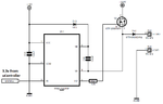
I'm having some trouble driving the MOSFET in attached circuit.

What I want to do is to have the MOSFET act like a switch that connects and disconnects the drain voltage to the load.

I'm driving the gate driver IC from a GPIO of an STM32 micro but I never get an output to the load, as expected.

If someone who has previous experience with this kind of application could help me understand what is going on here, I would highly appreciate it.

Thank you in advance.
 

Attachments

  • bootstrap drive.png
    bootstrap drive.png
    45.5 KB · Views: 273

Not sure what the load is and if it's compatible with bootstrap power supply operation. D14 will however "reliably" prevent circuit operation. To charge the bootstrap capacitor, node VS must be periodically pulled down to ground, e.g. by a resistive load.


Please also consider that the flyback pulse of an inductive load can destroy the driver IC, you probably want a diode between output and AGND. Try this circuit

bootstrap drive.png

- - - Updated - - -

P.S.: I was partly mistaken about D14 operation in the original circuit. It would (almost) allow a resistive load to pull down node VS. So a possible explanation for circuit failure is that the load isn't able to pull down VS and respectively doesn't charge C45. Or are you trying to drive the output permanently? That's not possible. The circuit can't drive the output statically, it can only drive a PWM duty cycle < 100 % to the output.
 
  • Like
Reactions: th_sak

    th_sak

    Points: 2
    Helpful Answer Positive Rating
Dear FvM,

Thank you for your message.

I have tried what you suggest with the diode but the result is the same. Still no output.

The load is for the moment an electronic load, but in the real app, it wiil be an SLA battery.

I want static operation (like a relay) but I have also tried with various duty cycles and I had no luck.
 

O.K., battery has initial voltage that prevents charging of the bootstrap capacitor. Also static operation of the driver isn't possible.
 

Hi,

A SLA won't work, because it prevents the bootstrap capacitor to be charged.
You need additional circuitry.
Either an isolationg DCDC converter, then you may use 100% duty cycle
Or a circuit that pulls down VS.

Debug:
* Use static HIGH drive signal
* use a DMM
* connect DMM_minus to COM of the driver.
* then use the other DMM wire to measure the voltage of each other driver pin.
* tell us all 5 voltages you measure

Klaus
 

Yes it sounds like your application isn't compatible with bootstrapping because of both the load and static operation. The bootstrap cap is like a tiny battery and it needs to be periodically recharged by having Vs pulled to ground (and we're talking more than once a second typically).

An isolated supply such as this will solve your problem by providing continuous power to the high side.
https://www.mouser.com/ProductDetail/CUI/PCSA1-S12-S12-S?qs=NPAmerw/ZTu9/vyVc9Ng0A==
 

Hi, and thanks to everyone.

It is clear that this aproach will not work for my app, so I'm thinking two other approaches.

1) Use an isolated DC/DC converter module like asdf44 has suggested.

2) Use a simple flyback converter to have an isolated gate voltage.

What do you thing about my options?

Are they any good, or there are some other better approaches to this problem?

@KlausST: The voltage to both HO and VS pins, with respect to ground is around 6V. The voltage to VB pin is around 11.5V and the signal from micro is 3.3V.
 

Hi,

1) VS and HO is the same: this means "not switching, no activity"
2) VS and HO about 6V: The bootstrap capacitor can't charge fully. Floating voltage supply will be in "undervoltage state". It will refuse to work.
3) VB 11.5V: non switching, no activity
4) IN = 3.3V: measured? Should be OK.
5) Vcc is missing.

DCDC vs flyback:
Did you compare cost and effort for both solutions?
Do you have a clue about expected average current? If not --> there are application notes how to estimate/ calculate the current.
Look at Mosfet manufacturers or driver manufacturers internet pages for related documents.

Klaus
 

am i getting something wrong here because it looks like you are wanting to switch the 250V on and off into the 12v (?) SLA battery so as to charge it?

Surely you should use a buck converter....and drive the high side fet with either a pulse transformer, or have an isolated supply for the hi side fet drive.
 

Hi again,

@KlausST, the voltage a Vcc pin was obvious, because it was mentioned at the schematic and I have also confirmed it with the DMM, but how should you know!

Anyway, I will use an isolated DC/DC power supply.

Actually I have already done it and works as I wanted to (static operation like a relay).

I was wrongly assumed that the bootstrap IC would work in static ON and OFF operation.

@treez, I didn't say a 12V volt SLA. By saying SLA battery, I had in mind my application, in which I consider "the battery" as 18 SLA batteries connected in series.

I consider the case closed and I will mark it as closed.

Thank you all guys.
 

Hi,

but how should you know!
True.
When one wnats to verify a circuit: nothing can be expected to be obvious. One always has to check. Best: directly at the IC pins - not at at the PCB... this enables to recognize soldering errors.

Klaus
 

Status
Not open for further replies.

Similar threads

Part and Inventory Search

Welcome to EDABoard.com

Sponsor

Back
Top