Continue to Site

Welcome to EDAboard.com

Welcome to our site! EDAboard.com is an international Electronics Discussion Forum focused on EDA software, circuits, schematics, books, theory, papers, asic, pld, 8051, DSP, Network, RF, Analog Design, PCB, Service Manuals... and a whole lot more! To participate you need to register. Registration is free. Click here to register now.

How to reduce input referred noise of an amplifier

Status
Not open for further replies.

student14

Member level 2
Joined
Sep 12, 2018
Messages
49
Helped
0
Reputation
0
Reaction score
0
Trophy points
6
Activity points
428
I want to reduce input referred noise of an op-amp more specifically of an OTA. OTA is to be designed for low frequency filter. For low frequency as fc = gm/CL, therefore for low frequency I need low gm value. Due to this small gm my noise is very high around 900uV/sqrtHz. How can I reduce this input referred noise.
In literature I have seen circuits designed with very low noise below 10uV/sqrtHz or even in nV/sqrtHz. I am designing a bulk driven OTA as attached but input referred noise is very high.

Any suggestions for reducing Noise. I have tried increasing the length for low flicker noise. I have also used PMOS differential pairs but still noise is quite high.

I am replicating the circuit shown in figure attached taken from one research article.

I have also tried to simulate the noise of core OTA as shown in figure2 attached. Reason for using core OTA to reduce noise coming from the cascode loads so I just kept considering the core OTA. But as source degeneration MOS is used of high Resistor value around 10M ohm. the gm of core OTA is very low in 30 nA/V. How to reduce this Noise Any suggestions?
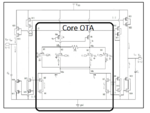
Core OTA.png
 

Having a higher gm with feedback may reduce the noise..
 
  • Like
Reactions: d123

    d123

    Points: 2
    Helpful Answer Positive Rating
Thanks for replying. But for low frequencies we need low gm. Gm with feedback means feedback should be an internal feedback. I am using source degeneration which also produces negative feedback.
 

Thanks for replying. But for low frequencies we need low gm. Gm with feedback means feedback should be an internal feedback. I am using source degeneration which also produces negative feedback.

Of course degeneration is a kind of feedback.It improves also the non-linearity.
 

Input equivalent voltage noise source is all your transistor noise current sources (i²_n=4kTGgm+F(i)gm²/f, where G is gamma_n - noise coefficient ≥0.5 and F(i) is a flicker noise coefficient (for some transistors can be proportional to the square root of drain current)) divided by the input device transconductance.

So, to minimize the input referred noise you should to minimize a transconductance of transistors in current mirrors and maximize input stage transconductance. The degeneration of input pair decreases its transconductance so increases noises. The solution here could be a play with current ratio between input and output branches.
 
  • Like
Reactions: d123

    d123

    Points: 2
    Helpful Answer Positive Rating
I have tried increasing the length for low flicker noise. I have also used PMOS differential pairs but still noise is quite high.
You can decrease Flicker with the increasing of the area! Length is not enough, because it decreases the gm of diff.pair. Degeneration also decreases, and feedback doesn't reduce the input referred noise, read about it in Razavi's book.
If the thermal noise is the problem, you have to increase the currents to increase diff.pair's gm, and the load capacitors too, then fc shouldn't change (or cool it down, rarely possible).
Special noise reducing technique is the active noise canceling (mainly for AC amplifiers), and the choppering (DC amplifiers do it well, it removes the offset, but clock is required). Research for these.
 
  • Like
Reactions: d123

    d123

    Points: 2
    Helpful Answer Positive Rating
There is one more issue the equivalent input noise is higher and the output noise is lower of the core OTA (highlighted in the diagram above). It means the Gm is less than 1. Its 30nA/V. I think for low frequency the Gm will be low especially when using source degeneration R = 10M. Gm = gm1/1+(gm1 * R) . Input noise of core OTA will always be high and output noise will be low. Then how to consider noise because output noise/gain = input referred noise. How to then find the input referred noise?

This is what I have understood. Please let me know if I am wrong?
 

I don't understand your issue, but if the output noise is less than the input referred noise that means your voltage gain is less than 1.
It doesn't mean that the Gm is less than 1, that isn't the gain.
 

If GM is very low then we need output R to be very high in giga ohms for the core OTA. To get high gain and thus low noise.

My issue is for the core OTA my circuits input referred noise is quite high and output noise is low. I want to reduce this. I have already used cascodes for increased output R to increase rout for high gain
 

Sorry, but how can be your output noise lower than input noise if you have high voltage gain? I assume you did something wrong, because it is not possible I think.
 

Yes I have tried to increase output R by using cascades to get high gain but my gain is still less than 1. And I am getting low output noise and higher input noise.

I.e. my GM is 30nA/V and ROut is in Mega ohms. And my over all gain is less than 1. Gain=gm ROut. How can I further increase R out to get further higher output in Giga ohms
 

If you voltage gain is below 1 it means only that your circuit does not work at all. Check DC operating points. Show us your testbench too.
 

If you voltage gain is below 1 it means only that your circuit does not work at all. Check DC operating points. Show us your testbench too.

The circuit is attached. The circuit I am replicating is taken from one research article. I am just trying to simulate the core OTA. I cant understand wheres the problem.

Core OTA.png

gainckt.png
 

Did you calculate the differential gain from BULKs to the output? How much is that? How much is the DC voltage on the BULKs? I see 0V on both, so your PMOS input pair bias is wrong I suppose. The BULKs need higher DC voltage than the source for normal operation. Connect the V0 and V1 between the vdd node and the BULKs.
 

Thanks for your reply. VO and V1? are you talking about the DC input voltage applied at the bulks. I am just applying ac signal no DC voltage. Do I have to use DC voltage at the bulks?
 

Sure. Otherwise they won't work...
 

The definition of OTA is a circuit which has all nodes low impedance instead of input and output. Diode connected fets are creating low impedance nodes. Your circuit is not an OTA now, you need to add current mirrors showed in the figure from 1st post. Without this you will always have an attenuation instead of gain and thus input noise higher than output noise. Especially, you input is bulk driven stage with gm-starving, so the Gm of it is roughly equal to gmb_2-gmb_1 (the degeneration factor is very close to 1 so I omit it), which is a few times lower than gm of your diode load and gds of input pair due to biasing it in linear region. Currently, I can estimate your gain as -20dB (≈0.1V/V) and input thermal noise spectral density as 40pV²/Hz and output noise as 400fV²/Hz.
 

Thank you for your reply. I haven't biased the input in linear region. It's in subthreshold saturation.
How you are calculating output noise?. I am using g cadence but noise is higher in hundreds of uv/sqrtz. Yours is quite low in pico volts? Did you find this noise using the complete figure shown in post 1.
 

Vdsat ≈ 3·n·Vt, assuming room temperature (which is pointed in the screenshot) and common value of n for bulk cmos ≈ 1.5 your vdsat is ca 115 mV, while Vds of input devices is 100mV. They are in linear.

My estimation was done as following.
Drain current of load is 7.5nA, effective input stage Id is 2.5 nA, it results with 190nS of gm of diode connected nfets and 60nS for input devices. The input signal is provided for bulk terminals, so gmb is a transonductor and its value is commonly 0.1-0.2 × gm, so suppose gmb=10nS. Degeneration factor is then equal to 1+10nS×5MΩ=1.05≈1, so can be omitted.

The gain of the circuit is equal to K=gmb/gout=gmb/(gm_load+gm_in)=10n/250n≈0.04 V/V.
The thermal current noise at the output:
i²n_tot≈i²n_nfet+i²n_in≈4·k·T·n·(gm_in+0.5·gm_load)≈3.85e-27 A²/Hz
Equivalent input series noise:
e²n=i²n_tot/gmb² = 38.5 pV²/Hz
Voltage noise at output:
v²n=K²·e²n = 0.04²·38.5p = 61.6f V²/Hz

Above numbers are in square voltages per hertz. Equivalent in V/sqrt(Hz):
en≈6.2µ V/sqrt(Hz)
vn≈250n V/sqrt(Hz)

The calculations are only for thermal noise. I cannot guess the flicker noise coefficients for your process, also bandwidth of this guy is probably very low, so flicker noise can dominant, however the noise simulation should provide independent spectra for different noise components.

However, your OTA is incomplete as long as you will not add current mirrors to it, as it is shown on figure from post #1. Then, you will see any gain and thus low input referred noise.
 
  • Like
Reactions: d123

    d123

    Points: 2
    Helpful Answer Positive Rating
Thank you for your detailed reply. The results are based on-hand calculation which is very low. But when I am doing noise analysis in cadence including current mirrors my input noise is lower compare to output noise which Is OK. But still I am getting higher input referred noise around 140uV/sqrtHz. This higher IRN is an issue
 

Status
Not open for further replies.

Similar threads

Part and Inventory Search

Welcome to EDABoard.com

Sponsor

Back
Top