Continue to Site

Welcome to EDAboard.com

Welcome to our site! EDAboard.com is an international Electronics Discussion Forum focused on EDA software, circuits, schematics, books, theory, papers, asic, pld, 8051, DSP, Network, RF, Analog Design, PCB, Service Manuals... and a whole lot more! To participate you need to register. Registration is free. Click here to register now.

Protocol generation using MOSFETS

Status
Not open for further replies.

knikhil271083

Member level 2
Joined
Jul 17, 2012
Messages
45
Helped
1
Reputation
2
Reaction score
1
Trophy points
1,288
Location
India
Activity points
1,676
Hi Experts,
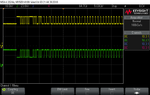
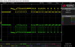
I am trying to generate a set of waveforms for my new project using a P-channel MOSFET. I am able to successfully generate the waveform. However, when I connect a load of only few mA (150mA) to it, the waveform dips.
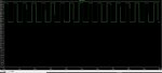
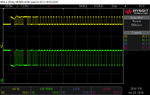
The protocol (waveform) is basically from a pedestal of 24V DC and above that there should be pulses of 6-9V DC. Simulation works fine, but when I built the circuit and loaded it, the loaded waveform drops below the pedestal. The maximum allowable load is about 800mA.
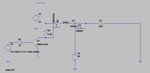
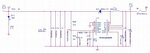
I have attached the LTSpice schematic for it. I have built the circuit using IRF9530 P-Channel MOSFET whose Id is more than 2A. I have observed the 34V supply & 24V supply, but they seem to be stable. Only at Drain of MOSFET, the pulse dips, dropping the protocol voltage.
I am not able to understand why this is happening.
Any help would be appreciated.

Regards
Nikhil
 

Attachments

  • Simulator_Protocol genrator1.zip
    699 bytes · Views: 92
  • Schematic.JPG
    Schematic.JPG
    39.2 KB · Views: 80
  • Waveforms.JPG
    Waveforms.JPG
    67.2 KB · Views: 69

Hi,

doing a simulation doesn´t mean you don´t need to read the datasheet.

V_GS max of the MOSFET is specified with +/-20V, but you drive it up to 34V. Maybe you´ve killed the MOSFET.
Additonally you may expect high voltage peaks coming from stray inductance caused by wiring (or load). Thus you should use an overvoltage protection across DS of the MOSFET.

Klaus
 

Hi,
Apologies for duplicate posts. When I first posted, it didnt appear in the forum. So I thought somehow it didnt get posted.
 

Hi,

Did a quick simulation with all supplies on 0.5R internal resistance. The 2222 base voltage is 0V to 5V, correct? Is this more or less what you see, at ~800mA an output voltage drop to 22.8V and peak of 32.6V?:

protocol generator person schematic.JPG

- - - Updated - - -

Hi there,

Do you think, if the 1N4007 voltage drop is about 1.4V, and that is the issue you describe..., that the problem may be the choice of diode - and worse, a little drop is inevitable with this series device circuit? In the simulation, by substituting the 1N4007 for a 1N5817 Schottky the output rises a little to 33.17V. Can the circuit be tweaked to substitute the diodes for MOSFETs with far lower forward voltage across DS than a diode, Schottky or not? ...If that's the problem...
 

Oof, good question. I'd suggest - with my limited experience - to look for a part with lower RDSon to begin with - the 9530 is not especially modern, good though it may be - and replace the diode with a second device with the same parameters. I don't know but I suspect it may be about reducing losses in the switch and diode however possible. Maybe another, more experienced member will disagree with the theory or provide a better (more practical) solution. With 34V, Zener gate protection is an issue to be dealt with unwillingly but necessarily...

- - - Updated - - -

...No chance of increasing the 34V by an equivalent amount to the expected voltage drop (1V to 2V to 35V or 36V)?
 

Hi,

Any pointers on how do I switch 34V using IRF9530?
Referring to your schematic of post #1:

* connect a 12V zener diode in parallel to R4 (this limits V_GS to a safe value)
* connect an additional 3k3 to Q1_collector (to limit the current)

*****
To get less V_DS voltage drop you may use a MOSFET with less R_DS_ON

*****
other solutions:
* You may use an integrated high side switch. (doing all the level conversion for you. Some come with other features like overcurrent protection, overvoltage protection, overtemperature protection, diagnostic output...)
* you may use a high side MOSFET_driver_IC and an N-CH_MOSFET.

I recommend to go through some reliable documents. Best are application notes of semiconductor manufacturers. (not random internet schematics)

Klaus
 
Paralleling the MOSFET by first a second and then a third one did nothing at all useful. By replacing the IRF9530 with the e.g. FDD4141 and the series 1N4007 diode with another FDD4141 the output rises to a theoretical 33.57V, a 400mV improvement on the Schottky version but still "far" from 34V. I'd seriously look at a similar type of MOSFET with around 12 to 18milliOhms RDS on (although the hard to comprehend 4141 RDS graphs seem to differ somewhat from the specifications...).

I personally feel that it is looking at the problem from the wrong end, if hateful voltage subtraction/theft is inevitable in the real world, no amount of wishing for a miraculous solution will compensate for that odious fact so it may be wise to see if a voltage can be added at the MOSFET switch output to compensate for both voltage drops (tricky/finickety sounding approach) or if possible and preferably by a long shot, increase Vin from 34V to [34V + expected voltage drop].
 

Have you considered an alternative solution: a regulator (LM317 for example) with it's ADJ pin controlled by the input signal. You lose a small voltage but the current capability is there and it only has to switch up to 9V so dissipation would be low.

Brian.
 

The behaviour described in post #1 doesn't fit the shown circuit. How can the loaded voltage fall below the "pedestal" voltage which is maintained by the 24V source and D3? If the transistor is turned on correctly, the pulse voltage drop won't be above D1 forward voltage + Iload*0.3. D1 isn't needed at all, b.t.w. For maximal load current of 0.8 A, there's no need for a lower Rds transistor, I believe. Limiting Vgs to a safe value of e.g. 15 V is however absolutely required
 

Hi,

Hope you've found a solution to the issue that is acceptable.

While not necessarily a solution to the problem of the voltage drop for a couple of reasons, I saw this today from an email newsletter advert and it's a nice looking IC and I thought maybe it might be of interest to get ideas or just to see what it can do and how it works MAX16141 3.5V to 36V Ideal Diode Controller
 
Hi All,
I was able to identify the problem and resolve them. There were two issues:
1. MOSFET biasing: I used the solution given by KlausST and it worked. The gate voltage now is around 17V (half of 34V due to two 3.3K voltage divider). So the MOSFET now works within its specs and switching waveforms properly.
2. Drop in voltage: The 34V was derived from 24V using a switched mode booster IC. While building the circuit, I had used an inductor available at hand. Its saturation current rating was around 120mA (too small for my requirement). I changed that to an inductor with current rating of 2.5A. Second change I did was the capacitor at 34V output. It was 47uF/50V electrolytic. I increased it to 220uF/50V.
(How I found it was 34V: I disconnected as booster and connected a bench top 34V supply of 0-2A rating. After slowing increasing the load above 100mA, I found that the current consumption on 34V started exceeding 120mA which was saturation current of the inductor I used. So I tested my full load with bench top power supply with modified circuit of MOSFET and it worked perfectly fine.)

I am now testing with the booster circuit connected with new inductor. I will post the results of testing here in a day or two if I run into further problems.

Thanks for all your support.

- - - Updated - - -

Have you considered an alternative solution: a regulator (LM317 for example) with it's ADJ pin controlled by the input signal. You lose a small voltage but the current capability is there and it only has to switch up to 9V so dissipation would be low.

Brian.

Hi Brian,
Seems interesting. I had used LM317 to limit current in one of my earlier project. What is say is definately worth trying. I will check the datasheet for some reference circuit and its compatibility for 34V.
Thanks
Nikhil

- - - Updated - - -

Paralleling the MOSFET by first a second and then a third one did nothing at all useful. By replacing the IRF9530 with the e.g. FDD4141 and the series 1N4007 diode with another FDD4141 the output rises to a theoretical 33.57V, a 400mV improvement on the Schottky version but still "far" from 34V. I'd seriously look at a similar type of MOSFET with around 12 to 18milliOhms RDS on (although the hard to comprehend 4141 RDS graphs seem to differ somewhat from the specifications...).

I personally feel that it is looking at the problem from the wrong end, if hateful voltage subtraction/theft is inevitable in the real world, no amount of wishing for a miraculous solution will compensate for that odious fact so it may be wise to see if a voltage can be added at the MOSFET switch output to compensate for both voltage drops (tricky/finickety sounding approach) or if possible and preferably by a long shot, increase Vin from 34V to [34V + expected voltage drop].

I agree. It was not totally OFF but the main problem was in 34V supply. Although MOSFET circuit is now improved.
Thanks
Nikhil
 

Hi,

the solution given by KlausST and it worked. The gate voltage now is around 17V
My solution was to use a zener diode to limit gate voltage. And I still recommend this.
The resistor divider may work for clean signals, with the given voltages...but the zener works in any case.

2. Drop in voltage
For your next problem:
* please post the complete circuit (this problem seems to be in a part of the circuit you dudn't show us)
* and don't post (unverified) informations like: "I have observed the 34V supply & 24V supply, but they seem to be stable."

Self made switcher circuit:
* increasing the capacitor value often gives no benefit. The better is to use capacitors with low ESR. --> see the swtcher datasheet
* according your description you used the DC input current (120mA) as saturation identifier. But in a switcher circuit there are (high) peaks at the inductor current ... which you have to consider as the saturation current. --> this also is described in the switcher datasheet.

You say you are still testing: Take care with the switcher PCB layout. It is critical. All is written in the datasheet.

Klaus
 

Hi,
I have attached the circuit of boost regulator using TPS55340. Datasheet of the Inductor L14 and capacitor C147 is also attached.
 

Attachments

  • 34V Boost Regulator.JPG
    34V Boost Regulator.JPG
    71.2 KB · Views: 70
  • Inductor_ihlp25cz-240021.pdf
    146.8 KB · Views: 70
  • Cap_e-uwt-880115.pdf
    323.8 KB · Views: 57

Hi,

I didn´t go through the datasheets.

But at first I was confused about your schematic. Usual signal flow is from left to right.

Klaus
 

Hi,
I tested with the boost converter circuit with full load. At 130mA, the waveform is clean. As I start increasing the load current, there is a droop in the first pulse of around 2V. I have attached the waveform. I have also observed that the waveform at the gas of the MOSFET also droops correspondingly.
Yellow waveform is the MOSFET switched voltage and green is at the gate of MOSFET. I am also attaching the circuit for reference. The MOSFET is question is Q6 at top left of circuit.
Any suggestions on this?
 

Attachments

  • Waveform_130mA.png
    Waveform_130mA.png
    23.4 KB · Views: 76
  • Waveform_550mA.png
    Waveform_550mA.png
    31.3 KB · Views: 55
  • Waveform2_550mA_.png
    Waveform2_550mA_.png
    26.4 KB · Views: 58
  • Mosfet switching.pdf
    273.9 KB · Views: 66

Hi,

What's exactly your load? A motor perhaps?
Measure the true current with a scope. I don't think it's clean steady 130mA.

Klaus
 

Gate voltage is set by Z-diode and can only drop if 34V input voltage is dropping. Unfortunately it's not shown in the waveforms, also the voltage source is unknown. In other words, the problem is beyond the scope of this thread.
 

Hi,

What's exactly your load? A motor perhaps?
Measure the true current with a scope. I don't think it's clean steady 130mA.

Klaus

I will measure the current output of the current sensor amplifier LT6100 on scope and will post the waveform. The load are addresable smoke detectors which communicate with the controller using pulses over 24V pedestal.
 

Status
Not open for further replies.

Similar threads

Part and Inventory Search

Welcome to EDABoard.com

Sponsor

Back
Top