T
treez
Guest
Hi,
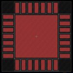
We are doing the PCB footprint for the 6x6mm QFN version of the PIC16F18856.
The recommended land pattern , on page 664 of the datasheet gives no recommendation for solder resist masking.
As such, we have put absolutely no solder resist anywhere under the body of the part. This is because we believe that solder resist would hold the part up off the board during reflow, and prevent proper settling of the part onto its pads. Do you agree with this?
Even if we put solder resist beneath the part, the gap between centre pad and outer pads is too narrow, and so we would get smatterings of solder resist over the pads, which would make the part even less likely to properly settle on its pads during reflow....do you agree?
The land pattern dimensions and the solder resist mask are shown attached.
PIC16F18856 datasheet
https://ww1.microchip.com/downloads/en/DeviceDoc/PIC16LF18856-76-Data-Sheet-40001824D.pdf