Continue to Site

Welcome to EDAboard.com

Welcome to our site! EDAboard.com is an international Electronics Discussion Forum focused on EDA software, circuits, schematics, books, theory, papers, asic, pld, 8051, DSP, Network, RF, Analog Design, PCB, Service Manuals... and a whole lot more! To participate you need to register. Registration is free. Click here to register now.

Smashing/customizing footprint of a component in Eagle Layout

Status
Not open for further replies.

Vaughn

Junior Member level 2
Joined
Feb 8, 2013
Messages
23
Helped
0
Reputation
0
Reaction score
0
Trophy points
1,281
Location
India
Activity points
1,520
Is it possible to smash down the footprint of any given component while working in the Eagle layout editor? I want to increase or decrease the distance between two footprint of a Resistor, can it be done without going through component library and by creating another package? Any trick are ULP available in the Eagle to do this?
kindly see the Attachment.
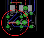
Increasing pad distance.png
 

Hi,

There are some solutions for this problem:
1) we created a jumper_wire device with many package variants. All packages with increasing distance in step size of 1/10 inch (2.54mm). In the board just use the "change package" comma d for different wire lengths. This is visible in the schematic and automatically creates an entry in the BOM. Good solution.

2) You may create a device with just one pad. Then place two of those pads anywhere you like in the board. Manually draw a wire at the tPlace layer to show the jumper_wire. You may use it on one single signal (which leaves an "unrouted wire" in the board for a correct assembling plan), or you may use it on different signals (then manually add a "jumper wire" in the schematic. This is a flexible solution, but it is not perfect because you need to manually add wires in board/schematic. It (wrongly) creates two BOM entries.

3) Use two vias in the board. Mind that they need the tStop and bStop openings to make them solderable. This creates no visible solution in the schematic, thus I recommend to add this manually. You may use this solution on one singke signal (which keaves an unrouted wire), or you may use it on different signals.
I also recommend to add the jumper wire in the board for a correct assembling plan.
This is the most error prone solution, because (without manual editing) it is invisible in the schematic and you may miss to add the xStop openings. No entry in the BOM.

If you use solution 2 or 3, then you may use an extra "signal layer" (layer2 ... layer14) to insert the connection. This avoids the "unrouted wire" at a random position. This is useful when both wire connections use the same "signal".

Klaus
 
  • Like
Reactions: Vaughn

    Vaughn

    Points: 2
    Helpful Answer Positive Rating
Status
Not open for further replies.

Part and Inventory Search

Welcome to EDABoard.com

Sponsor

Back
Top