jktheone1987
Newbie level 3
To verify the gain boosted, I design this easily to understand models which are as follows.
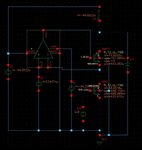
Fig.1 is the common gate amplify structure,

Input source is bottom voltage source V19 which has AC and DC signal shown below

Both two transistors are in saturation region and I add an inductor with inductance of 10PH to treat as an AC block in order to investigate the maximum gain the transistors can give.
Gain boosted structure is realized by a ideal amplifying structure, with the parameters showm below

This gain parameter will vary from 10 to 10K to test the boosted outcomes.
Plus input and reference output are set to make sure the two transistors are operating in a saturation situations.
Sweeping the gain of gain booster amplifier, the outcomes are

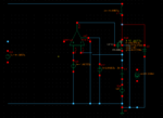
However, I design an similar structure which is common gate amplifier, which is shown below.

Input source in V24, with AC magnitude 1V, and the current sink is to make sure the gain boosted amplifier will not deterioate the operating point of main MOS NM6, the current is 44.6uA. Other conditions are the same, the outcomes are

I think the outcomes should follow the same rountine: the higher the gain of gain booster, the higher the whole gain, why these two are different and the first one reaches an upper boundary. I really do not know why the up limit exists in the first one.
Thank you.
Fig.1 is the common gate amplify structure,

Input source is bottom voltage source V19 which has AC and DC signal shown below

Both two transistors are in saturation region and I add an inductor with inductance of 10PH to treat as an AC block in order to investigate the maximum gain the transistors can give.
Gain boosted structure is realized by a ideal amplifying structure, with the parameters showm below

This gain parameter will vary from 10 to 10K to test the boosted outcomes.
Plus input and reference output are set to make sure the two transistors are operating in a saturation situations.
Sweeping the gain of gain booster amplifier, the outcomes are

However, I design an similar structure which is common gate amplifier, which is shown below.

Input source in V24, with AC magnitude 1V, and the current sink is to make sure the gain boosted amplifier will not deterioate the operating point of main MOS NM6, the current is 44.6uA. Other conditions are the same, the outcomes are

I think the outcomes should follow the same rountine: the higher the gain of gain booster, the higher the whole gain, why these two are different and the first one reaches an upper boundary. I really do not know why the up limit exists in the first one.
Thank you.