mmwicant
Newbie level 5
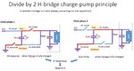
Divide by 2, H-Bridge, step-down, switched-capacitor, charge-pump - Operation principle of is shown the attached jpg.
Suppose we look at node “bottom”.
In steady-state it toggles between voltages (Vin+ε)/2 and 0V, while Vout is at ~(Vin-ε)/2.
i.e. the bottom right transistor experiences OFF and ON states in opposite polarities !
The involved voltages are >>5V so NMOS and PMOS are asymmetrical, due to the multiple wells that enable the high VDS operation.
For example for PMOS:
VSD>0 and VSG>Vth => Isd>0 (ON state)
VSD>0 and VSG<Vth => Isd~0 (OFF state)
But when VSD<0 regardless of VSG, the diodes between Drain and Bulk will conduct.
I.e. reverse SD polarity enable current through diodes.
Should the Bottom Right switch be realized by a PMOS?
And if yes, do you agree it will run negative direction current through the its diodes?
Is it OK?
Should it work like that?