Continue to Site

Welcome to EDAboard.com

Welcome to our site! EDAboard.com is an international Electronics Discussion Forum focused on EDA software, circuits, schematics, books, theory, papers, asic, pld, 8051, DSP, Network, RF, Analog Design, PCB, Service Manuals... and a whole lot more! To participate you need to register. Registration is free. Click here to register now.

[SOLVED] EM Simulation of GSG Pads

Status
Not open for further replies.

Puppet123

Full Member level 6
Joined
Apr 26, 2017
Messages
356
Helped
22
Reputation
44
Reaction score
21
Trophy points
18
Activity points
3,059
Hello,

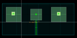
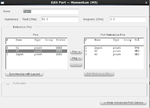
I am designing GSG pads for probing RFIC/MMIC and want to simulate this in Keysight Momentum.

What type of port type do I use - point ? Do I place it in the middle of the pad where I will probe? The edge of the pad? Is it an edge type port ?

Thanks.
 

Pin/port position determines the reference planes, so I place it where the probe tip touches down.

gsg2.PNG

gsg1.PNG
 

Hello Volker@Muelhaus,

Thank you for your message.

In that screenshot you sent - is the signal pad on the top metal and the gnd pads are on all metal layers via-ed down to the "blue" layer - which I assume is ground ?

Is this correct ?

Thank you.
 

In that screenshot you sent - is the signal pad on the top metal and the gnd pads are on all metal layers via-ed down to the "blue" layer - which I assume is ground ?

Yes, the blue layer is Metal1 and used as a ground plane in this transmission line case. In other cases (e.g. inductors) there is no ground plane, and the vias are connected down to the substrate.
 

Hello Volker@Muelhaus,

The GND pads you are using in that set up - they are going from Top metal through to all the metals down to the gnd metal layers - so all metal layers on top of one another and then down to metal 1 - with many vias ?

Thank you.
 

The GND pads you are using in that set up - they are going from Top metal through to all the metals down to the gnd metal layers - so all metal layers on top of one another and then down to metal 1 - with many vias ?

Yes, to make the via connection you also need the intermediate layers.
 

Hello Volker@Muelhaus,

What layer are your port pins on - are they all on top metal ?

Thank you.

- - - Updated - - -

Hello Volker@Meulhaus,

Here is a copy of my simulation in Momentum.

Wondering if you can comment on it.

I have 3 three pads, two on sides, on top metal via-ed all the way down to ground plane in blue with vias - flattened to speed up simulation.

Middle pad, signal pad, with top metal only.

Middle pad, connect to microstrip transmission line with M9 signal layer and M1 ground, same as blue ground plane.

Ports all on top metal - set up in momentum - signal pad port is positive, two ground pads are negative.

What is wrong - the results are nonsense.

Thank you.
 

Attachments

  • GSG.png
    GSG.png
    9.7 KB · Views: 338
  • GSG_Ports.png
    GSG_Ports.png
    18.5 KB · Views: 342
Last edited:

Yes, pins on top metal. What you describe sounds correct to me. No idea what goes wrong in your case. Have you checked current density view to see the current path?
 
No, its working fine, my mistake.

Thank you.
 

Status
Not open for further replies.

Part and Inventory Search

Welcome to EDABoard.com

Sponsor

Back
Top