Continue to Site

Welcome to EDAboard.com

Welcome to our site! EDAboard.com is an international Electronics Discussion Forum focused on EDA software, circuits, schematics, books, theory, papers, asic, pld, 8051, DSP, Network, RF, Analog Design, PCB, Service Manuals... and a whole lot more! To participate you need to register. Registration is free. Click here to register now.

MMWave Layout/EM Simulation Questions

Status
Not open for further replies.

Puppet123

Full Member level 6
Joined
Apr 26, 2017
Messages
356
Helped
22
Reputation
44
Reaction score
21
Trophy points
18
Activity points
3,059
Hello,

I am laying out am amplifier that operates around 100 GHz.

I want to EM simulate the interconnect of the transistors (metal stacks and vias) so I can capture the inductance, resistance and capacitance - my understanding is that the common extractors for parasitics do not capture the inductance properly, so I would like to EM simulate them.

My layout involves stacking many layers of metal (it is a silicon process, I am using the top metal of a 7-8 metal process as my signal metal) through many vias.

My question is: I was told that HFSS would be the way to do this due to its' 3D nature, but I am wondering whether Momentum would be adequate even though it might not capture the vias properly (I could use 3D via modeling with Momentum but it takes forever I find, maybe I am doing it wrong). Also would Momentum capture the skin effect properly at these frequencies ? Would the edge meshing be accurate - can or should I increase the meshing of the edge meshing ?

Does anyone have any thoughts or experience with these EM issues for the transistor layout parasitics due to interconnects especially over 60GHz ?

Was not sure whether this posting was best posted in this forum or the Analog IC Layout forum. I decided to post it here since it is more EM related.

Thank you.
 
Last edited:

I was told that HFSS would be the way to do this due to its 3D nature

The people who told this are (a) HFSS sales people or (b) don't have a good understanding of EM tools. 3D planar tools like Momentum have some advantages for this type of work when it comes to port definition.

but I am wondering whether Momentum would be adequate even though it might not capture the vias properly (I could use 3D via modeling with Momentum but it takes forever I find, maybe I am doing it wrong).

Momentum can do the vias accurately.

For some RFIC work you might want to merge via arrays into larger via boxes, to reduce simulation time. This requires some attention to (a) avoid unphysical x-y currents on merge via arrays and (b) avoid increasing the effective via array cross section (-> via resistance). If you REALLY care about via details, for transistor detail modelling, I recommend to not use via array merging.

Also would Momentum capture the skin effect properly at these frequencies ? Would the edge meshing be accurate - can or should I increase the meshing of the edge meshing ?

Using edge mesh is fine and gives accurate results. Without edge mesh, the side wall mesh will take currents that push to conductor edges.

Does anyone have any thoughts or experience with these EM issues for the transistor layout parasitics due to interconnects especially over 60GHz ?

Yes, using Sonnet and Momentum and 3D FEM. The main challenge is proper definition of ports here, i.e. good understanding of what port parasitics you introduce by what port type.
 
Last edited:
Hello Volker@muehlhaus,

Thank you for your reply.

I will say that every academic peer reviewed research paper and research thesis I have seen uses a "3D simulator" like HFSS, EMPro, Keysight/Agilents old FEM simulator to do this task and says it is "required".

Also, I was told Momentum is a 2.5D simulator and thus "inadequate" for this task.

Just sharing what I was told and have read, just want to make sure I do it right and capture what I need to capture.

Thank you.
 
Last edited:

I know what you mean, but these people usually have limited understanding of EM tools.

Here is an example of some transistor level EM work at 80 GHz using 2.5 D Sonnet that I supported a while ago:
https://ieeexplore.ieee.org/document/6140934/

nils1.PNG
 

Hello,

Thank you for you reply.

Also another question: is transmission line meshing required in this situation ?

Also you mention ports - ports definition and parasitic of ports.

Typically I use edge ports/pins in momentum - is this a correct approach here ?

What do you mean by parasitics I introduce by the port ?

Thank you.
 

Also another question: is transmission line meshing required in this situation ?

I use transmission line mesh for nice 3D current views with precise current distribution, but it doesn'make much difference for S/Y/Z-parameter results.

Also you mention ports - ports definition and parasitic of ports.
Typically I use edge ports/pins in momentum - is this a correct approach here ?

Yes, that's fine in Momentum. The issue is mostly with lumped ports in 3D EM, that really have a lot of internal parasitic inductance from path length inside the port. Luckily, that issue doesn't exist in Momentum.
 
Hello,

Thank you again for your reply.

I had some questions about the link you posted.

In the link you posted: Effect of ground cutout size on RFIC inductor performance, you use an inductor of diameter 105um. You simulated a cut out of up to 30um.

Again, I was "told" that the rule of thumb (read it in a thesis, who claimed it was a rule of thumb with no evidence) is the ground distance is 1/2 the diameter - or in your case it would be about 50um.

Since inductance gets closer to the created value of 500pH, as the cut of distance increases, is this a good rule of thumb - it would depend on the application obviously, ie. LNA, Mixer vs VCO where you might not get that distance.

Thank you.
 

Again, I was "told" that the rule of thumb (read it in a thesis, who claimed it was a rule of thumb with no evidence) is the ground distance is 1/2 the diameter - or in your case it would be about 50um.

Yes, I agree. For inductor simulation in Sonnet with a closed metal boundary around the inductor, I even recommend box size = 3 * inductor diameter, to minimize the influence.

In the appnote, I wanted to show what happens at small distances. The distance is a trade-off between ground frame influence and chip area.
 
Hello,

Thank you for your reply.

I had an additional question about HFSS solve inside vs. Momentum Edge Mesh.

HFSS users have claimed to me that HFSS is better at handling skin effect at very high frequencies due to solve inside and thus they say HFSS is best for planar type structures.

My question is: is edge mesh as good, better or worse at capturing skin effect over 60GHz than solve inside using HFSS or besides HFSS any other simulator ?

Thank you again.
 

HFSS users have claimed to me that HFSS is better at handling skin effect at very high frequencies due to solve inside and thus they say HFSS is best for planar type structures.

If they claim this, ask them to provide proof.

From my 20 years experience in EM, Momentum's skin effect modelling ist perfectly fine, if you allow a dense enough mesh. And I have seen many HFSS users create poor RFIC models with bad port configuration and poor results. But it's not my job to sell Momentum, so anyone is free to use whatever he trusts in. If you think HFSS is great, and your colleagues have had good results, go for it!
 
Last edited:

Hello,

Thank you for writing.

I am not here to argue for products or sell them, I am just learning and learning the limitations and capabilities of types of simulators. Concepts stay, while companies come and go. New simulators will come and go, but they will use the same basic techniques.

I was pointed to this paper, when I asked for proof: https://ieeexplore.ieee.org/abstract/document/7369151/

Paper doesnt explain the setup though, so I take it with a huge grain of salt.

As I said, I am not arguing for a product or selling it. Just want to learn the capabilities, limitations and usefullness of each simulation technique (FEM, MOM, FDTD) and their variants (2D, 2.5D, 3D).

What density of meshing have you found works well ? I use about 15 sometimes. Is that too small ?

Thank you again.
 

I was pointed to this paper, when I asked for proof: https://ieeexplore.ieee.org/abstract/document/7369151/

I can't access the paper, but I worked with this group at TU Dresden on transmission line EM modelling for IHP BiCMOS PDKs. At that time, they used Sonnet 2.5D EM and Sonnet indeed has an issue because it can't model currents on the conductor side walls. Instead, Sonnet uses a multi-sheet workaround that in my opinion is not very good for practical cases. So I would indeed expect 3D EM to do better there than Sonnet.
Momentum does accurate side wall currents with the same mesh resolution that is also used in the x-y plane, so that aspect is fine in Momentum.

I recently did a bit of transmission line modelling using 3D FDTD (Empire XPU) and included the conformal passivation etc, which isn't possible with the 2.5D tools. That model with fine volume mesh provided very decent agreement for loss and phase, actually better than what I got from Momentum. Testcase is 750um line length in IHP SG13S.

SG13_750nm_S21dB.PNG
SG13_750nm_S21phase.PNG

- - - Updated - - -

What density of meshing have you found works well ? I use about 15 sometimes. Is that too small ?

In Momentum, I use 20 cells per wavelength (i.e. large compared to geometry dimensions) and edge mesh for normal accuracy requirements. Depending on the size of the DUT, I also limit the mesh size to an absolute value like 20µm.

In the inductor ground cutout appnote, I used transmission line mesh with 5 cells + edge mesh to have a very detailed current density for the plots. It didn't make much difference in results, but looked nicer. But don't trust me on this - you should do your own testcases because your models & requirements might be different.
 
Last edited:
Hello,

Thank you again for your reply.

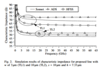
I am attempting to make microstrip lines with side shields (one of topics of this paper) so these issues are important to me. I put some of the text in paper below and a screen capture of one of the figures.

They compared HFSS, Momentum and Sonnet in it for side shielded transmission lines amongst other topics.

So edge ports are fine then ? And since the line is shielded - if I am using metal 9 of a nine metal process as my signal layer and metal 4 as my ground for the microstrip, then I reference the port to Metal 4 (neg port in momentum) and pos port to metal 9. The side shields are via-ed to the ground plane, say Metal 1.

I hope this set up is correct.

Thank you again for your assistance.

--

From paper:

By adding grounded side walls in the layout of microstrip lines, the field characteristics of the line can change dramatically with decreasing distance s to the side walls; text-book estimations for calculating the characteristic impedance of transmission lines are not valid anymore; for equations for shielded coplanar waveguide and shielded microstrip lines.

Depending on the conductivity of the metal layers in use, the return current of the line is forced to flow into the top-most metal of the side walls and the characteristic impedance is lowered in comparison to a conventional microstrip line because of the higher capacitive coupling to the ground.

When modeling this hybrid structure in an EM simulator, this behaviour introduces further difficulties. In Agilent Advanced Design System (ADS) and
ANSYS HFSS the definition of the ports used in simulations can have a very high impact on the simulation results, while in Sonnet the top-most metal layer has to be simulated with sufficient amount of sublayers within the metal.

Fig. 2 shows the simulation results of the proposed line with widths w of 3 μm (TL1) and 10 μm (TL2) and side wall distance s of 10 μm of the three above mentioned EM simulators. These simulations already show a variation of the characteristic impedance of about 10 % between the simulators.

Moreover the trend of the characteristic impedance is not deterministic between the simulators and therefore cannot be predicted in advance.
 

Attachments

  • TLines.png
    TLines.png
    28.6 KB · Views: 178
Last edited:

Interesting. For your case, I would then recommend to use transmission line mesh + edge mesh combined. As you can see in the 3D mesh preview, this will refine mesh on both x-y plane and side walls.
 
Thank you,

Does my port set up sound correct ?

Thanks again for your help.
 

Please show a screenshot of layout with pins, and pins to port mapping, to avoid misunderstanding what your setup is.

Port calibration: For RFIC work, I disable port calibration in Momentum. From my experience, the line calibration method doesn't work well with lossy silicon underneath.
 
Thank you,

I got my port set up figured out.

Thank you for clarifying this, many have told me that for over 30 GHz planar structures (passives, interconnect), HFSS is the way to go, and Momentum will not give adequate or accurate results and I should not even contemplate using Momentum.

Thanks again for your help.
 

Volker,

Does EMpire XPU show a good agreement between simulation and measurement for planar structures ( coils,filters,couplers etc.) regarding to your past experiences ??
 

Hello,

@Volker or @BigBoss - Is FDTD the preferred simulation approach for EM simulation of broadband interconnect and passive strictures, ie. for optical broadband circuits and other wideband circuits that operate on time domain signals (like square waves) ?

I have limited experience with FDTD.

Thank you.
 

Volker,

Does EMpire XPU show a good agreement between simulation and measurement for planar structures ( coils,filters,couplers etc.) regarding to your past experiences ??

I did some extensive benchmarking using Empire XPU for IHP SG13S for transmission lines and inductors, with very good agreement to measurements.
I still use Momentum often because that gives accurate results in many cases. I use Empire for those cases where the FDTD method is more efficient (on-chip antennas with local backside etching or RFIC layout with very large polygon count that "hits the wall" for MoM/FEM meshing)

- - - Updated - - -

Is FDTD the preferred simulation approach for EM simulation of broadband interconnect and passive strictures, ie. for optical broadband circuits and other wideband circuits that operate on time domain signals (like square waves) ?

All of the methods - MoM and FEM and FDTD - have their strength & weaknesses.

As you have found yourself, HFSS FEM is well known and widely used when it comes to non-planar work like packages.
I have very good experience with MoM for many planar simulation tasks in RFIC: accurate and efficient.
One advantage of FDTD is that it scales very nicely where you go to large analysis volumes (large in wavelength), so FDTD is very efficient for on-chip antenna work at >100GHz.

So all these tools can be useful in RFIC work.
 
Status
Not open for further replies.

Part and Inventory Search

Welcome to EDABoard.com

Sponsor

Back
Top