Continue to Site

Welcome to EDAboard.com

Welcome to our site! EDAboard.com is an international Electronics Discussion Forum focused on EDA software, circuits, schematics, books, theory, papers, asic, pld, 8051, DSP, Network, RF, Analog Design, PCB, Service Manuals... and a whole lot more! To participate you need to register. Registration is free. Click here to register now.

SPWM converter mosfet failure

Status
Not open for further replies.

Dimitrisvlamis

Member level 2
Joined
Dec 12, 2017
Messages
42
Helped
1
Reputation
2
Reaction score
1
Trophy points
8
Activity points
366
Greetings,

I am currently working in this circuit of an SPWM inverter and i keep having my mosfets buring after each time i conect the ceter tap to the transformer! I am running out of ideas, mosfets and...money haha :lol: The circuit is pretty simple. The code works, i tested it from arduino without mosfets. I generate spwm signals (no signal is on each other) with frequency of 50Hz and pwm frequency of 15000kz. My input is 12V and i use an iron transformer 8-0-8 to 220v taken from a UPS. Any sugestions why my mosfets burn? asd.PNG
 

Hi,

What kills your Mosfet:
1) overvoltage on gate-source (even peaks in the microseconds)
2) overvoltage on drain-source (even peaks in the microseconds)
3) overcurrent on drain (even short peaks)
4) overtemperature of the silicon

1) and 2) can be obsered by connecting a (differential) voltage probe as close as possible to the Mosfet pins.
The peaks may come from stray inductance/ bad PCB layout.
Mind that V_DS will be (needs to be) at least 2 x VIn. Any higher voltage may be suppressed by suitable overvoltage protection devices.
3) May be caused by too high load current, cross conducting of both Mosfets
4) May be caused by not sufficient heatsink, or too high power dissipation. Too low gate drive voltage or too slow gate drive rise and fall rate.

Show us your PCB layout.

Klaus
 

How exactly the source current of Q1/Q2 returns to the negative of C3 filter cap? I can't see a path for GND on the layout.
 

How exactly the source current of Q1/Q2 returns to the negative of C3 filter cap? I can't see a path for GND on the layout.

I have 2 holes left and right to connect 2 thick wires to the ground so that ground is as as close to MOSFETs
 

Hi,

This is why usually a single sided PCB layout is not sufficient to make a reliable high currrent high frequency switching circuit.

Just a connection from A to B may work in simulation and in a schematic, where the connecton is considered to have zero impedance.
But on a real circuit there is ohmic resistance and - sometimes even worse - impedance caused by stray inductance.

The signals become dirty, with overshoot and ringing. Peaks of high voltage may occur. Switching speed becomes slow and discontinous which causes increased heat in the MOSFET.

Usually every semiconductor manufacturer for power switching devices provides and application notes and other informations on how to design a suitable PCB layout. They explain what you need to take care of. --> Read through them.

My recommendations to try to make your circuit working:
* A thick wire from C5_GND tor R3_GND
* a 30V MOV across each MOSFETs drain-source. Very short connections.
* C9 will cause a lot of current during switching transitions. Decrease it´s value and/or include a series inductance .. combined with a sutable RC combination to suppress LC resonance effects..
* Add 100nF ceramics capacitors directly at each supply pin to GND pin of each IC. Short wiring.
* add a (big) bulk capacitor at the input of your 7805. It´s more important than big capacitors at the output.

*****
Genrally:
* read throuch standard PCB design rules: especially distance of trace to outline.
* use useful isolation distance: reduce the distance with your low voltage signals
* use useful isolation distance: increase the distance with your high voltage signals. Proper saftey distance for 230V AC to other non related voltages is >6mm!! (area of D3..D6)
(Don´t use GND around these high voltage signals.)
* be sure to use resistors with enough voltage rating plus safety margin for R8, R9

Klaus

- - - Updated - - -

Hi,

I have 2 holes left and right to connect 2 thick wires to the ground so that ground is as as close to MOSFETs
Ok - I see.
Mind: shorter signal paths are better than thicker wires. (high frequency impedance is about independent of wire gauge)

***
I also recommend to have all three transformer primary windings connections on your PCB. This enables twisted wiring, which reduces stray inductance. Additionally you may connect a fast capacitor to GND.

Klaus
 

Hi,

This is why usually a single sided PCB layout is not sufficient to make a reliable high currrent high frequency switching circuit.

Just a connection from A to B may work in simulation and in a schematic, where the connecton is considered to have zero impedance.
But on a real circuit there is ohmic resistance and - sometimes even worse - impedance caused by stray inductance.

The signals become dirty, with overshoot and ringing. Peaks of high voltage may occur. Switching speed becomes slow and discontinous which causes increased heat in the MOSFET.

Usually every semiconductor manufacturer for power switching devices provides and application notes and other informations on how to design a suitable PCB layout. They explain what you need to take care of. --> Read through them.

My recommendations to try to make your circuit working:
* A thick wire from C5_GND tor R3_GND
* a 30V MOV across each MOSFETs drain-source. Very short connections.
* C9 will cause a lot of current during switching transitions. Decrease it´s value and/or include a series inductance .. combined with a sutable RC combination to suppress LC resonance effects..
* Add 100nF ceramics capacitors directly at each supply pin to GND pin of each IC. Short wiring.
* add a (big) bulk capacitor at the input of your 7805. It´s more important than big capacitors at the output.

*****
Genrally:
* read throuch standard PCB design rules: especially distance of trace to outline.
* use useful isolation distance: reduce the distance with your low voltage signals
* use useful isolation distance: increase the distance with your high voltage signals. Proper saftey distance for 230V AC to other non related voltages is >6mm!! (area of D3..D6)
(Don´t use GND around these high voltage signals.)
* be sure to use resistors with enough voltage rating plus safety margin for R8, R9

Klaus

- - - Updated - - -

Hi,


Ok - I see.
Mind: shorter signal paths are better than thicker wires. (high frequency impedance is about independent of wire gauge)

***
I also recommend to have all three transformer primary windings connections on your PCB. This enables twisted wiring, which reduces stray inductance. Additionally you may connect a fast capacitor to GND.

Klaus

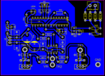
DSADSDSAD.PNG

First of all thank you so much for the reply. So I redisgned the Board, i added 100nF to every supply (atmega, max4427, 7805 and ceter tap) i tried to eliminate jumper wires , i put MOVs between Drain-Sources and i put the center tap on the pcb. TR1 TR2 and TR3 are the transformer windings. What do you think about this version? Any commennts on this? Thanks in advance once more.

- - - Updated - - -

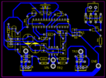
δασ.PNG

And this is a design without ground plane
 

Hi,

much better now.

But C20 isn´t really close to the VC pin (pin 7). --> place C20 more close to pin7.

******
Some information about how to design EMI/EMC compliant PCBs.

Every current flow needs a closed loop.
The job of C20 is to stabilize the voltage on VCC of the microcontroller.
But the microcontroller´s (HF) current flow is on VCC (pin7) and GND (pin8).
Now draw the loop for the current flow: pin7 --> C20(+) --> C20(-) --> pin8
EMI_EMC.PNG
In your case it is more than 150mm in length (with a very narrow connection close to pin15).
The max outline dimension as about 50mm, which makes it sensible to noise in the low GHz area (WiFI, Cellular phone, Bluetooth...)

The enclosed area is about 800mm^2, which is a measure how much energy this "antenna" can receive/transmit.

Now if you place C2 close to pin7 and pin8:
The max dimension length is about 10mm, which shifts the "antenna frequency" to about 5x higher frequencies.
But most important the encolsed area now is reduced to less than 50mm^2.
Which means it can not receive/transmit much energy.
******

i tried to eliminate jumper wires
There´s no need to eliminate jumper wires. This is not the target.
Your target should be to generate a solid GND plane, without cuts and traces....Usually impossible with a single layer PCB.

For a two layer PCB this means: (sooner or later you can´t go with 1 sided PCBs - not in a professional environment)
* GND plane - without additional wiring - on one side
* all the wiring on the other side. No need for copper pour on this layer.

Klaus
 

In SPWM inverter if you use center tapped inverter you may have to do dead band shorting. Why don't you try H bridge ?. Later if you want to scale up the capacity also it will be useful.
 

And this is a design without ground plane
In my eyes: You never had a true "ground plane". You had a copper pour. But this far away from being a GND plane.
With a GND plane you never have current loops in the length of 150mm, and the return path is usually exaclty on the opposite side (layer) of the current carrying traces, which means the enclosed area is very small.

This results in
* stable signals
* low EMI
* good EMC

Klaus

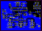
AASDS.PNG

Thanks, I put the C20 where you suggested and rearranged some stuff. This is how it looks now.

- - - Updated - - -

What is dead band shorting? I've never heard of it. I didn't find anything in google. I want to use this because if i use H bridge i will have to use High Side switching and connect the transformer windings in parallel. It will be more complex if something happens, i can troubleshoot center tap topology easier in my opinion.
 

I don't quite understand what you want to say. But I've seen this design working in action. What do you mean by reactive power?
 

I do not like the look of that C9 across the secondary, it
seems prone to take a -lot- of charge at 2u*200V and
will reflect a very low impedance to the primary on every
switching edge.

The only possible thing it could be good for is EMI / snubber
duty, but snubbers always have a series R.

Easy enough to lift one lead and see if stuff quits stinking.

I was testing it without the capacitor and same thing happened. This cappacitor is to filter the output of the transformer to make the waveform more like a sinewave
 

When one primary winding is energized, do you see a voltage generated in the other (idle) primary winding? It may generate a brief spike, at a high voltage able to damage a mosfet.
 

My suspicion is simply that the iron cored transformer isn't suitable for use at 15KHz an presents too low an impedance for the MOSFETs to drive. I think this is a 50Hz step down transformer being used in reverse and simply may not be suitable for high speed pulsing, even if it is modulated at 50Hz.

Brian.
 

It normally works but the transformer has to be split bobbin type to achieve higher leakage inductance.
I have seen couple of such designs. Temperature will be slightly in the higher side and efficiency will be lesser.
 

It normally works but the transformer has to be split bobbin type to achieve higher leakage inductance.
I have seen couple of such designs. Temperature will be slightly in the higher side and efficiency will be lesser.

What are you suggesting me to do? I will try lower the frequency of the PWM but i dont see why this shoulb be a problem. I am saying again this is a transformer taken from a pure sine UPS
 

As you turn off your MOSFET there will be a reverse current from the transformer. In H bridge that is normally passed through the free wheeling diodes.

- - - Updated - - -

No need to lower the PWM frequency, you need to make some arrangement to manage the reactive power during turn OFF. Kindly refer the other inverter whether they have dead band shorting MOSFET's also the pwm frequency.
 

Status
Not open for further replies.

Similar threads

Part and Inventory Search

Welcome to EDABoard.com

Sponsor

Back
Top