Continue to Site

Welcome to EDAboard.com

Welcome to our site! EDAboard.com is an international Electronics Discussion Forum focused on EDA software, circuits, schematics, books, theory, papers, asic, pld, 8051, DSP, Network, RF, Analog Design, PCB, Service Manuals... and a whole lot more! To participate you need to register. Registration is free. Click here to register now.

Explantion Required for an RF System

Status
Not open for further replies.

adnan012

Advanced Member level 1
Joined
Oct 6, 2006
Messages
468
Helped
2
Reputation
4
Reaction score
2
Trophy points
1,298
Activity points
4,923
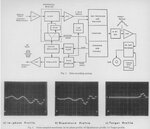
I need the explanation of the attached diagram. What is the working principle ?

What is the the delay block? How delay is achieved ?


The diagram is taken from the link.

***.semanticscholar.org/paper/A-Guided-Radar-System-for-Obstacle-Detection-Patfterson-Mackay/8a9776e710a4b0a432c48e4bf3da16f19f986e23
 

Attachments

  • 3-Figure3-1.jpg
    3-Figure3-1.jpg
    197.6 KB · Views: 140

I think delay block is to sync the transmit signal with receive signal to account for time of flight of the signal. For method of delay block, I would assume a circulator may be used. It clearly is a radar detection system, but blocks in it are too ambigious to decide what exactly it does.

Guess: It seems like a I-Q mixer at the receiver end. So, delay block gives a selection between I and Q of mixer, depending on application.
 
Thanks for reply.

Suppose we have a pair of parallel 100 meter slotted /leaky coaxial cables separated by 2 meters. A spectrum analyzer is attached the one cable and the other end is terminated . The first cable is driven by a continuous 100MHz sine wave. In second case, we drive the cable with 250nSec pulse modulated with 100MHz , and the pulse rate is 50/sec.

What we will observe at the receiving side cable attached to spectrum analyzer and/or spectrum analyzer?
 

Status
Not open for further replies.

Part and Inventory Search

Welcome to EDABoard.com

Sponsor

Back
Top