skatefast08
Full Member level 3
So, a while back (some of you might remember me from my queries on the design I was making for an LNA), I designed a microwave pre-amp (LNA) at 2.4 GHz with an ATF-55143 transistor and had it manufactured and tested it on a VNA. My expected results were: a max S21 of (negative)-18.3 dB at 2.31 GHz, a minimum S11 of -20.5 dB at 2.48 GHz, and a minimum S22 of 18.95 dB at 2.38 GHz. My test results came out with responses for an S11 a minimum of -10dB at 1.58 GHz, S21 was achieved a maximum of 10dB at 1.55 GHz, and S22 had a horrible response of basically 0 dB all throughout the frequencies, and BW = 100 MHz.
I am sure my matching circuits were correct, to match a 2.4 GHz pre-amp. I would be pleased to give you the values of my L matched networks, so that you could check for me if I designed it correctly. I have attached a picture of my circuit diagram below to show you the matched networks. The s-parameters for bias point at Vds=3V and Id = 30mA is as follows (s2p format): 2.4004 0.60735 -127.6034 7.4564 85.6026 0.061004 29.8354 0.47717 -57.9411. You can also check on the datasheet for the s-parameters as I have posted in the next paragraph.

Schematic
The s2p file that I used for my design had a bias point of Vds = 3V and Id = 30mA, which I believed my Vgs = 0.6V, which is shown in an IV graph on the datasheet, which you can download from this website in pdf: . So, I used a voltage divider to get Vgs = 0.6V, which I assumed my Vds would equal to 3V and Id would be 30mA; would this be the wrong or correct way of going about the problem? So, when assuming my Vds = 3V and Id = 30mA, I calculated a resistor value to go between Vdd = 5V and Vds = 3V and got roughly 67 Ohms.
CIRCUIT RESULTS:
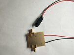
I also believe my results could have turned out bad, because of bad soldering, but I don’t know if that would have made that big of a difference or not either. A picture of my LNA frontside and backside(ground) are shown below.
.jpg")
frontside

backside (ground)
DC TEST RESULTS:
I also tested the voltages and current and got: Vds = 2.36V, Id = 38.2 mA, and Vgs = 0.6 V. What did I do wrong, to achieve Vds = 3V and Id = 30mA? The schematic is shown above.
MOST IMPORTANT QUESTIONS I HAVE:
What did I do wrong, to achieve Vds = 3V and Id = 30mA?
Would the bias point significantly have changed my LNA resonant frequency to 1.55 GHz and create a mismatch at the output (S22) also for a 1.55 GHz pre-amp?
Could the big splotches of solder at the bottom have made a big difference to create large parasitics at the ground? Also, some of the vias were accidentally filled with solder as shown in the pictures.
Would my L matching networks using lumped components have been a problem too, or did I design incorrectly the L matched networks?
I am sure my matching circuits were correct, to match a 2.4 GHz pre-amp. I would be pleased to give you the values of my L matched networks, so that you could check for me if I designed it correctly. I have attached a picture of my circuit diagram below to show you the matched networks. The s-parameters for bias point at Vds=3V and Id = 30mA is as follows (s2p format): 2.4004 0.60735 -127.6034 7.4564 85.6026 0.061004 29.8354 0.47717 -57.9411. You can also check on the datasheet for the s-parameters as I have posted in the next paragraph.
Schematic
The s2p file that I used for my design had a bias point of Vds = 3V and Id = 30mA, which I believed my Vgs = 0.6V, which is shown in an IV graph on the datasheet, which you can download from this website in pdf: . So, I used a voltage divider to get Vgs = 0.6V, which I assumed my Vds would equal to 3V and Id would be 30mA; would this be the wrong or correct way of going about the problem? So, when assuming my Vds = 3V and Id = 30mA, I calculated a resistor value to go between Vdd = 5V and Vds = 3V and got roughly 67 Ohms.
CIRCUIT RESULTS:
I also believe my results could have turned out bad, because of bad soldering, but I don’t know if that would have made that big of a difference or not either. A picture of my LNA frontside and backside(ground) are shown below.
frontside
backside (ground)
DC TEST RESULTS:
I also tested the voltages and current and got: Vds = 2.36V, Id = 38.2 mA, and Vgs = 0.6 V. What did I do wrong, to achieve Vds = 3V and Id = 30mA? The schematic is shown above.
MOST IMPORTANT QUESTIONS I HAVE:
What did I do wrong, to achieve Vds = 3V and Id = 30mA?
Would the bias point significantly have changed my LNA resonant frequency to 1.55 GHz and create a mismatch at the output (S22) also for a 1.55 GHz pre-amp?
Could the big splotches of solder at the bottom have made a big difference to create large parasitics at the ground? Also, some of the vias were accidentally filled with solder as shown in the pictures.
Would my L matching networks using lumped components have been a problem too, or did I design incorrectly the L matched networks?
Attachments
Last edited: