Continue to Site

Welcome to EDAboard.com

Welcome to our site! EDAboard.com is an international Electronics Discussion Forum focused on EDA software, circuits, schematics, books, theory, papers, asic, pld, 8051, DSP, Network, RF, Analog Design, PCB, Service Manuals... and a whole lot more! To participate you need to register. Registration is free. Click here to register now.

Having troubles properly simulating a rectifier in ADS

Status
Not open for further replies.

LouieM

Newbie level 3
Joined
Jun 19, 2018
Messages
4
Helped
0
Reputation
0
Reaction score
0
Trophy points
1
Activity points
41
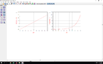
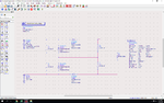
Hello I am an undergrad student and was given the task of designing a rectenna in ADS with very little knowledge of how to use ADS or microwave design so and guidance in this would be so helpful. I guess my main issue is that I have built the rectifier that I designed in ADS and my results do not match at all. Also I performed a power sweep on the circuit and an it seems like the dBm out exponentially increases as pin increases. I read online that there will be a saturation point then decay. Can you see anywhere in my circuit that is wrong that may be causing this issue.

Thank You
Lou
 

Attachments

  • PSWEEP.png
    PSWEEP.png
    78.8 KB · Views: 100
  • FWVD.png
    FWVD.png
    107.2 KB · Views: 101

The ideal components that you have used in simulation don't exist in real life. For the large capacitor values, real components have much different behaviour at your operating frequency than the ideal parts. Do the real life check: Take one of your capacitors, go to the network analyzer and measure capacitor S11 from DC to your operating frequency.
 

I'm confused about the values of our capacitors not existing. We are using values of the caps used in our real world circuit. Is there a better way to model them in ADS? I only ask because our professor would like our experimental results to be close to our simulated. Am I wasting my time trying to do this? I'm confused about the last part. Sorry my knowledge of microwave circuits is very limited. I just stared undergrad research at my new university and have had very little help from my professor or his grad students.
 

I'm confused about the values of our capacitors not existing.

Your caps with 22 µF have a low self resonance frequency and will have massive losses at your operating frequency, or is that 0.22µF?
 

The capacitors on the left are .22uF and the ones on the right are 100uF. What would be more appropriate for these values?
 

I guess my main issue is that I have built the rectifier that I designed in ADS and my results do not match at all.
Is a schematic truely matched to actual measurement ?

Especially, Connections of "PORT1", "Term2", "C3" and "C5" are correct ?

Also I performed a power sweep on the circuit and an it seems like the dBm out exponentially increases as pin increases.
Can you understand "dBm()" ?
"dBm()" is nonsense for "vout".

And your circuit is a rectifier, so you should observe vout[::,0] not vout[::,1].

Show me netlist or schematic for Power Sweep.
 

I'm pretty sure that they match, I've went over both the circuit and schematic so many time to try to fix my problem. Ive attached a picture of my circut but it may be hard to follow. Your right, I am kind of confused why dBm is used.
I changed vout[::,0] to vout[::,1] and the graph didn't change

Thank you for taking your time to help me with this. It is extremely appreciated!
20180720_124503.jpg
power sweep.png
 

I'm not at all familiar with circuit design for the RF range, but I would say that the above assembly at the breadboard (which has a lot of metallic strips inside) along with the aerial wirings, can be a significant factor on screw up the validity of any simulation for 170MHz, but I may be wrong. Anyway, I would consider grounding the surrounding unused lines of the breadboard close to the mounted parts (which should be grouped together), just for shielding purpose.
 

The high frequency part of the circuit have to be developed keeping the wiring between components as short as possible. I'm referring to C3, C4, anode of DIODE1 and DIODE3, cathode of DIODE2 and DIODE4. Thus they cannot be simply accomodated on a strip breadboard.
Furthermore I don't understsand the 50 ohm termination connected to C4. It shoud be instead connected to ground.
In a real circuit you have to connect a coaxial cable from generator to C3 (inner conductor) and C4 (shield) and also you should connect a 50 resistor (using short leads) between the input of C3 and C4 in order to match the generator output.
Another thing. You have to plot the voltage across the load, that is across R1, you instead plotted the output of DIODE1 referred to ground, that is wrong. To do this you have to name also the net on the other side of R1 (for instance VoutG) and plot Vout-VoutG vs. time.

I think that, roughly, the circuit should start to rectify at a generator output power of about 15 dBm
 
Last edited:

170 MHz is start of RF range. U need to trim those legs of the lumped components you are using. Caps should be soldered together and connections should be made smaller. If that's a regular breadboard your total signal path seems like 50cm or so. You did not even trimmed the legs of diodes ( which should be working in 170MHz according to your schematic). Look at wavelength and signal path interference concept in RF frequencies.

Forget about those jumper wires. Point of circuit is not being pretty.

Use SRF concept to calculate the working limits of your lumped components. At 170Mhz the caps you use may be acting like inductors.
 

Status
Not open for further replies.

Part and Inventory Search

Welcome to EDABoard.com

Sponsor

Back
Top