Continue to Site

Welcome to EDAboard.com

Welcome to our site! EDAboard.com is an international Electronics Discussion Forum focused on EDA software, circuits, schematics, books, theory, papers, asic, pld, 8051, DSP, Network, RF, Analog Design, PCB, Service Manuals... and a whole lot more! To participate you need to register. Registration is free. Click here to register now.

[SOLVED] Bias Tee configurations

Status
Not open for further replies.

ktr

Full Member level 3
Joined
Jun 11, 2018
Messages
165
Helped
17
Reputation
34
Reaction score
16
Trophy points
18
Location
Ireland
Activity points
1,433
Hello all,

I am designing a LNA to place right after an antenna to minimize the cable loss( also to deal with mixer products on later stages) induced into my receiver chain. I'm planning to place this LNA in a small-box right near the antenna for efficiency. Since starting this, I have seen a lot of Bias-tee conversation about it; but I'm confused of what is the difference between a Bias Tee and a normal RF choke.

I searched around but failed to found a resource to learn how to design a bias tee in schematic, or draw one on a layout.
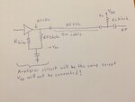
Rf choke.jpg
Normally I would just use a RF-choke like this, but I am having a hard time imagining what would a seperate bias-tee would look like.

Any suggestions or help is welcome.

Best Regards,

ktr


---

Edit: My frequency is about 4Ghz.
 

bias T design can range from very easy to near impossible depending upon the bandwidth and power requirements.
In your case, assuming fairly narrow band operation it should straight forward.
As you realise you need a high shunt impedance at teh operating frequency across the transmission line. The 0.5nH inductor you show will be difficult to realise physically. Use a quaterwave high impedance line instead of the inductor. Use as thin a track as you can realibly fabricate and that will handle the DC current, about 100 ohms should do. Use a suitabe capacitor to RF ground the track, taking into consideration the parasitic and mounting inductance (a few pf). A radial stub or similar would also do for the RF, backed up by some larger capacitors to decouple any LF noise that may be on the DC.
If you buy a bias T it will be an inductor capacitor configuration as you have drawn but for a wider bandwidth the inductor could well be conically wound to reduce the parasitics allowing the use of a higher value without resonance than would normally be the case. the grounding capacitor would be a wide band type, again with low parasitics to reduce inband resonances.
 

Hello G4BCH,

Actually I found some 0402 package fixed inductors from mouser.com (given in link) quarter wave TL would be too long for my case(I calculated the distance)
https://www.mouser.com.tr/datasheet/2/400/nductor_commercial_high-frequency_mlg0603s_en-918291.pdf and they are for my normal RF choke in circuit(part of matching circuit, not with bias-tee)

Ok, thinning the TLine for a "better" open in RF is a trick I know, will do that. 5nH at 4 Ghz is roughly 130ohms. I understood this topology from what you said, is it correct ?

bias-tee.jpg

Kind Regards,

ktr
 

The 5nH inductor and making use of the self resonance is a good way to go.
I would not worry too much about the thin line you show, just place the 'live' mounting pad for the inductor directly the signal track to absorb the stray capacitance.
 
  • Like
Reactions: ktr

    ktr

    Points: 2
    Helpful Answer Positive Rating
This inductor I choose has SRF @20 GHZ, and it should have a ~120 130 ohm reactance coupled with "thin" line, I assume would be enough of a choke for bias-tee. Ok, in layout I will place one of the inductor ports as close as to coax line, I will remember that when drawing it.


I have heard about this SRF trick before but never used myself.
Are you saying I should use a inductor to resonate around my working band? What value of reactance would it show in that scenario? :)
 

Assuming an ideal inductor 125ohms at 4GHz is 5nH. Looking at the data sheet you reference the self resonant frequency of a 5nH inductor is around 5GHz, not 20GHz, so you will be usign the SRF.
The impedance of the choke will be much higher than 125 ohms, just what you want. As to what it will be that will depend on the parasitics, but in this case with a Q of about 5 it will be around 600 ohms, quite high enough not to have any significant effect on a 50 ohm system.
Using the SRF of an inductor in bias circuits is quite common, you just need to be mindful that you are dealing with a parasitic tuned circuit and not just and inductor, it can cause problems as well as solve them.
The inductor pad wants to be on the track rather than close to it, in that case the pad is absorbed in the track and has no effect on the circuit; otherwise you have to account for the extra tracking. That will help to get rid of the strays you don't want and keep the ones that can be made to work for you.
 
  • Like
Reactions: ktr

    ktr

    Points: 2
    Helpful Answer Positive Rating
Whoa, thanks for the information. Now, I understand how it works.

Putting the pad on track is confusing me on layout drawing part though. I deduce that I should make this bias-tee on the same pcb with my LNA. Most of commercial Bias-Tee's I have seen is a module by itself; but it would not work for my case If I understand it correctly, due to usage of SFR inductor and narrowband nature of my design I suppose.

I will add this bias-tee near the Output of my LNA PCB, with one of the inductor's legs on the pad and a DC-blocking capacitor for RF line but without the thin line in my drawing.

What value of resonance should I select for that LC circuit ? From top of my head, I can say a 33pf is about 1ohm near that Freq, and that LC circuit would have ~400 MHz Resonance freq. Should I be worried about that?

Best Regards,

ktr


P.S. Seriously, thank you for the information. I learned something new today.
 
Last edited:

Assuming that the image makes it through this is what I mean. The tracks are shown in blue and the pads are white.
I was making the assumption that you were going to use the bias to provide power for the LNA.
On the left hand side the inductor is mounted directly on the 50 ohm track so that the pad becomes part of it. On the right hand side the inductor is connected to the 50 ohm track via another track, this track and the pad become a complex stub attached to the line and will have to be accounted for in the design. For the C to ground you need a low impedance at the signal frequency, for 4GHz something around 3.3pf should be OK. Don't forget the parasitic inductance of the capacitor will cause a series tuned circuit, so a 33pF wil probably act as an inductor at your operating frequency. The SRF and impedance curves are given by some manufacturers. A ferrite bead or higher value inductor can be used between the HF decoupling and any LF decoupling that you need. That will help to reduce any parallel resonances between the capacitors.
The track beween the L & C adds to the inductance but does not affect the transmission line.

For the bias you want to avoid any resonances that are not going to help you, You need a high impedance for the L hence using the parasitic parallel resonance, and a low impedance for the C here using the parasitic series resonance. What you want to try to avoid is any resonance near the band of interest between the L and the C, that would cause a notch in the signal path.
Pads.JPG
 

To close the topic, I want to share what I did.

I built the Bias-tee(C5, C6, C7, C10 L3) on its own using your advices about it, left a place for another inductor if I need it. Downloaded the inductor's s-parameters from the manufacturer. It(bias-tee) has a s11 of -40db near DC, and -1.3db around 4Ghz.

I also simulated the LNA on its own(S11 near -25, S22 -15), and they both give good results. When I combine them into a single circuit though, I got some weird simulation results.

When the biasing resistor of my amp(R2 in picture) is deactivated in schematic, everything works smoothly. But when I activate it, S22 and gain detoriates(S11 and Stability is unchanged somewhat).
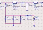
**broken link removed**

I lean to think ADS does not understand SRF impedance of inductor, hence it does not do the impedance matching correctly(I will learn how to do that asap). I expect it work nevertheless. I did the layout as you suggested, one of the pads of inductor is located on top of track, with the bypass caps behind it.

Kind Regards,

ktr
 

I agree with biff44; try 8.2 or 10nH with a capacitor of about 10pF. this should give a close to ideal bias T around 4GHz.
Modelling the S parameters a TDK 10nH 0603 inductor and 10pF 0603 capacitor (which do, or should take into account the resonances) directly across 50 ohms gives beter than 30dB retuirn loss and negligible insertion loss. Real life will be a bit worse.
 
  • Like
Reactions: ktr

    ktr

    Points: 2
    Helpful Answer Positive Rating
I got lost a bit in circuit schematic after I realized L2 becomes open because of Rbias in RF analysis; hence L2 has no effect on matching with this configuration. I need to connect Rbias to Vdd of amp, but its also the RFout of circuit.

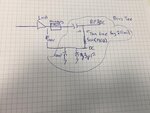
I thought maybe, I should split up bias-tee into the Rx side, like this; but I can not get the simulation results;; so I think I'm doing something wrong.
IMG_4789.jpg

lna_out.JPG
 

I'm gonna add a parallel Capacitance of 33pf to Rbias to solve that issue of openness of L2. So, in DC that Cap will be open and Rbias will supply LNA. In RF, that cap will short the Rbias to gnd; hence preserving my matching circuit.
 

Status
Not open for further replies.

Part and Inventory Search

Welcome to EDABoard.com

Sponsor

Back
Top