Continue to Site

Welcome to EDAboard.com

Welcome to our site! EDAboard.com is an international Electronics Discussion Forum focused on EDA software, circuits, schematics, books, theory, papers, asic, pld, 8051, DSP, Network, RF, Analog Design, PCB, Service Manuals... and a whole lot more! To participate you need to register. Registration is free. Click here to register now.

My first Eagle library for socket - request for validation

Status
Not open for further replies.

TheMartian

Junior Member level 3
Joined
Jul 6, 2018
Messages
28
Helped
0
Reputation
0
Reaction score
0
Trophy points
1
Activity points
322
Hey,
I have made my first Eagle library for RJ45 socket (I modified the other one), but I am not sure if I got this correctly.
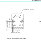
Can you please look at the datasheet and check if my pinouts are connected correctly?

Datasheet:
View attachment JXD0-0006NL.pdf
Library:
View attachment myEagleLibToCheck.lbr.zip
Screenshots (this RJ45 will replace old RJ45 connector which I don't have):
myRJ45Library_1.png
myRJ45Library_2.png
myRJ45Library_3.png
myRJ45Library_4.png
myRJ45Library_5.png
myRJ45Library_6.png
myRJ45Library_7.png
indatasheet.png
datashchema.png
It is imporatnt especially because I am going to order 10 PCBs from chinese manufacturer, so I kinda have one-shot and can't afford such mistakes.

I understand that both in datasheet and Eagle the connector is shown from top(component) side, is this right? Is my pins order correct?
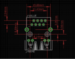
 

Hi,

I see a lot of issues. Some are minor with just a couple of 0.01mm, but others are far away.
I don´t know if some tolerance is OK for you. Technically it may be, but I recommend to exactly use measures given in the datasheet.

for P1...P7 I recommend to use:
grid mil 25 1 mm [Enter]
They all need to be placed on this grid.
all X positions are only a bit OFF, but the Y positions don´t match at all.
***

The big holes are too small.
Other are wider than in the datasheet (not that critical)
and many other issues.

****
I recommend to use the correct and useful grid and grid-multiplier.
Then it will be more visible if they are correct or not.

Switch between mm and mil, because some measures are mm related others are mil related.

use the INFO command and type in the correct X and Y postions directly.

****
For a raw validation you can print out the package with 1:1 scale then place the true connector on it.

Klaus
 
You are right, I have assumed that the new connector will have the same dimensions as connector I used as base (I copied other library), and only changed pin order.
I was wrong, so now I will correct the dimensions and check again.

Still, can you tell me if at least the pins order is correct?

Also, how do I move element by given offset in Eagle? I mean, I want to select P1-P8 and then move in Y. I tried using Group tool to select P1-P8 and type "Move 0 5" or "Move * 0 5" but it says "unknown pad"...
 

Hi,

Still, can you tell me if at least the pins order is correct?
use
SET pad_names ON [Enter]
to show the pad names. Then you easily can verify them vs the datasheet.

Also, how do I move element by given offset in Eagle? I mean, I want to select P1-P8 and then move in Y
for very small movements: (let´s say 0.00123mm down.) I use the input with values method:
* grid mm [enter]
* select P1..P8
* move [enter]
* move cursor to (0 0)
* right mouse click at (0 0)
* (0 -0.00123) [enter]
finished

****
for larger movements (lets say 12.123mm down), i use the move by hand with the help of grid method:
* grid mm 12.123 [enter]
* select P1..P8
* move [enter]
* move the cursor to where you like
* right mouse click
* move the curser (with the selected group) to the desired position. step size = grid size, thus you can`t go wrong.
* left mouse click
finished

Klaus
 
I have mostly improved it but I have one issue left.
The LED pins relation to the entire module seems off.
I can't really trace where is there error - it looks like that the entire part is not symmetrical (the one I am making or the one I used as base):
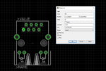
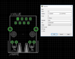
See:fixedENCsocket.png


My EAGLE file if you want to CHECK/SEE: View attachment v2_20180727.rar

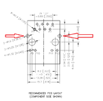
on the technical drawing, it seems that one of two holes is not exacly on the outline of the part:
fixedENCsocket2.png
is this drawing error or the parts are not really 100% symmetrical?
Can you help me?
 

Hi,

why don´t you move the LEDs to the correct position?

BTW: the 8 pads block is slightly off the 25 mil grid

I didn´t check all dimensions.

Klaus
 
I fixed LEDs and remaining dimensions, I hope this is final version, but can you recheck before I order gerbers?

BTW: the 8 pads block is slightly off the 25 mil grid

I can see that but I can't find any more dimensions//relations that are wrong


Here's current version:
finRJ45ihope.png

I changed everything I can think of, including the size of holes. They are a bit bigger just to be sure that everything will fit.

Here's lbr:
View attachment rj45_20180728rar.rar


PS: Why can I easily add hole dimension display for drill hole but I can't add it for those "green" holes with solder pads?
 

Hi,

Now it´s the third time you ask someone else to check the measures.
Still some values are off. Some only by small values (still the 8 pad block). Maybe this is OK for you, we don´t know.
Others are up to 0.44mm off. For my taste too much. (Front line of placeplan: 10.31mm vs 10.75mm)

--> You need to learn to do this on your own.

How I do it:
* Print out the 2 pages of the connector-PDF with the measures.
* use a green marker or any other green pencil
* measure by measure check if it is important for you. If it is not important then clearly cancel it out with the pencil.

* all remaining measures need to be cross checked with the EAGLE package.
* Use the EAGLE GRID setup "mil" to check all mil (inch) related measures.
* if there is a difference, then correct it immediately.
* use the pencil to clearly check every validated measure.
* Use the EAGLE GRID setup "mm" to check all mm (metric) related and other measures.
* if there is a difference, then correct it immediately.
* use the pencil to clearly check every validated measure.

* re check the two print out pages that every measure needs a mark. Either "canceled" or "checked".

*******
If you have a PDF viewer where you can paint in your own lines, you don´t need to print out on paper.

Klaus
 
Hi,
Now it´s the third time you ask someone else to check the measures.
Still some values are off. Some only by small values (still the 8 pad block). Maybe this is OK for you, we don´t know.
Others are up to 0.44mm off. For my taste too much. (Front line of placeplan: 10.31mm vs 10.75mm)

Thanks for review, but are you talking about the gray part outline?
You are right, 10.75mm, but I simply didn't check it, because only the holes matters for me. I just have enough space around connector on PCB.

I was asking about the holes only because I assumed that outline does not really have to 100% match yet.
 

Hi,

As already said: We don´t know what is important for you and what not.
For me the outlines are important, too. Especially the said (grey) front line, because with this I align the connector to the front panel.
And if other outlines are not correct you risk to place two parts close to each other... but when you want to assemble them they don´t fit....

Klaus
 

Status
Not open for further replies.

Part and Inventory Search

Welcome to EDABoard.com

Sponsor

Back
Top