Continue to Site

Welcome to EDAboard.com

Welcome to our site! EDAboard.com is an international Electronics Discussion Forum focused on EDA software, circuits, schematics, books, theory, papers, asic, pld, 8051, DSP, Network, RF, Analog Design, PCB, Service Manuals... and a whole lot more! To participate you need to register. Registration is free. Click here to register now.

Gating Signals for BSNPC inverter

Status
Not open for further replies.
Even if I increase the capacitance of C1 and C2 upto 1000uF, the output remains the same.
Do you mean I have to increase the frequency of the gating signals or do you mean something else?
 

I also tried using MOSFETs to do the job but the result was not plausible. I also tried to accomplish the same task with JFETs and "somewhat" got "some" result.

A hardware circuit should have resistors in the bias wires to the transistors.

The mosfet model in Falstad's simulator just happened to turn on okay with a 5V bias signal. Often it needs a higher voltage. It's unpredictable that way regardless of what threshold voltage I choose as a parameter.

Normally I use transistors in simulations because they are more predictable. By varying the bias resistor I can alter current through the transistor. Since it's current driven this makes it easier to get an idea whether current through the transistor has a complete path in the circuit.

The control circuit (the divide-by-2 flip flop and logic gates) is a project in itself. Try a simple simulation of that alone. Then it is easier to correct errors.
Once it's working correctly you can add the transistors. Etc.
 

Guys, I am getting desperate and I have tried every method provided and I am not getting any results.
I am getting short on time as I will have to present the project's progress to my supervisors before the end of this month and I am not confident that such progress, until now, will be acceptable by them:cry:.

I will be plenty happy if someone can guide me in the right direction.
 

Hi,

can we have a complete summary of your current state:
* simulation or real circuit?
* signal flow
* actual schematic
* signal flow (sources, scope pictures where the signals are OK, and scope pictures of where the signals are not as expected
* ... and so on


Klaus
 

Bidirectional switch neutral point clamped three-level inverter...

Could this be the intended waveform? (Found by internet search)

50 hz comblike to sinelike.png

- - - Updated - - -

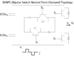
Here is another schematic (obtained by an image search for bsnpc).

BSNPC.png

- - - Updated - - -

And another schematic.

different bsnpc.png

The switching devices are arranged differently from your schematic posted earlier in this thread.

- - - Updated - - -

By adding the inductor at the output, it filters out the higher switching frequency. If you want a sinelike waveform at the load then it requires tailoring components to the proper values.
 
Could this be the intended waveform? (Found by internet search)

Yes that is what we require and isn't the configuration in the third image more like a half-bridge configuration.
As far as the tailoring is concerned, I have tried caps and inductors of different values in my previous config. I will try to implement the configs that you have provided and hope I will get some results.

I really appreciate the help you have provided so far, many thanks.

- - - Updated - - -

The post#12 depicts the circuit in real time but if you are able to get a vague idea, here is the image:
received_323807575059604.jpg
I used multiple arduinos to remove grounding problems (as previously described in older posts). I have not worked on hardware until then because I thought maybe getting some results from the simulation would prove helpful but I am having second thoughts about that now.
and this is the output from the circuit:
View attachment A0001DS.BMP
When given time and tightening the loose wires, the output looks like this:
View attachment A0002DS.BMP
The output's "supposed" negative pulses tends to increase in amplitude up to the positive pulses (i.e, the whole output looks like transitions only.

Unfortunately, I did not print that image from the oscillo.
 

Hi,

This is not a circuit for hardware beginners.
The photo shows lengthy wiring which causes stray inductance (a simulation doesn't know about this stray inductance unless you add these inductors). Thus your real circuit will differ from the simulation results.
The stray inductance causes ringing, maybe high voltage peaks...they easily can kill your semiconductors.

I strongly recommend to use isolated gate drivers instead of multiple arduinos.
(Multiple arduinos need very precise synchronisatiin, which can not be guaranteed)
For tests you could build your own isolated gate drivers: (for each Mosfet/IGBT)
* a small DCDC power supply module, maybe 12W, 1W
* a logic level optocoupler (or other logic level isolator)
* a gate driver IC like TC1412N (just as an example, there are many similar ones)
Connect them as close as possible to the Mosfets/IGBTs
This makes your live easier for the testing phase. Later you may replace them with more simple/cheaper circuits.

Klaus
 
Hi,
For tests you could build your own isolated gate drivers: (for each Mosfet/IGBT)
* a small DCDC power supply module, maybe 12W, 1W
* a logic level optocoupler (or other logic level isolator)
* a gate driver IC like TC1412N (just as an example, there are many similar ones)
So I have to use a 12V regulator and make a veroboard that would provide power to all gate drives and then use opto-coupler in between them, please refer to the image:
IGD.png

Ignore the multiple drives and couplers (just want to confirm if the circuit is correct).
 

As said: "for each MOSFET"

a 12 V regulator (7812) is not what I meant.
With 12V DCDC module I meant isolating modules. like AM1Dxx12, where "xx" is for the input voltage.
There are many other manufacturers and many other types of isolated DCDC converters.

And I said logic level optocouplers. In your schematic there are non_push_pull transistor outputs. It doesn´t work the way you´ve drawn it.
For sure there are many other ways....but I can´t give all possible soutions.

Klaus
 
Hello again everyone,

I changed my simulation a bit and I have tried to incorporate all the fixes that are recommended here.
Here is my simulation:
PC816_Schm.PNG
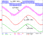
and the output:
PC816_Result.PNG

If you noticed, the output is obtained between the bi-directional and the half bridge MOSFETs.

If I try to simulate the circuit by using logic level opto-couplers, I do not get the required output:
Here is the schematic:
HCPL_Schm.PNG
The output:
HCPL_Result.PNG

As you can see, the HCPL is kind of clipping the positive part (I wonder why).
Please refer to https://datasheet.octopart.com/HCPL-2201-Avago-datasheet-8212218.pdf for the datasheet. I followed the implementation provided in the datasheet on page 15.

I have also implemented the circuit by using GaN transistors, for which I used the model import wizard, but I get analog node limit error whenever I implement the entire circuit.
Does anyone have a fix for that ?

Note: The implemented circuit is a 2-level inverter (of course not what I originally required:|)
 

I get analog node limit error whenever I implement the entire circuit.

1.
Your schematic has a 0V ground icon, with the only other connection being to an optoisolator. Hence the simulator may be unable to determine what current flows to ground, since your power supplies are not referenced to ground, but only between their own + and - terminals.

2.
The simulator may be unable to determine when to turn on M1 & M2. These have D1 & D2 in their source leg. The diodes are high resistance while they are Off. They conduct when the gate turns on the mosfet, and the gate needs to see a definite voltage at the source terminal in order for the mosfet to turn On. It creates a paradox for the simulator.

The error might go away if you were to put the diodes in the drain leg.
 

Hi,

... additional issues:
* first: please clean up the schematic. Avoid crossings. My recommendation: draw only one [mosfet, supply, optocoupler..] circuit. Then copy it. So that all 4 look the same.
* you overdrive the HCPL inputs
* all 4 optocoupler outputs need to be isolated --> you must not join their GNDs. All is individual. Only the power side of the Mosfets is connected.

Klaus
 

You are using unsuitable gate drivers in any schematic posted in this thread. Either use dedicated opto coupled gate drivers or fast logic opto couplers with separate gate driver ICs or discrete push pull drivers.

HCPL-0201 is a good fast coupler, but 20 mA output current isn't sufficient to drive power MOSFET, particularly pull-down the gate to prevent miller induced shoot-through in a bridge topology.
 
Status
Not open for further replies.

Part and Inventory Search

Welcome to EDABoard.com

Sponsor

Back
Top