Continue to Site

Welcome to EDAboard.com

Welcome to our site! EDAboard.com is an international Electronics Discussion Forum focused on EDA software, circuits, schematics, books, theory, papers, asic, pld, 8051, DSP, Network, RF, Analog Design, PCB, Service Manuals... and a whole lot more! To participate you need to register. Registration is free. Click here to register now.

[PIC] PIC12F519 communication protocol

Status
Not open for further replies.

saeedazari

Newbie level 5
Joined
Jun 5, 2014
Messages
8
Helped
0
Reputation
0
Reaction score
0
Trophy points
1
Activity points
69
Hi everyone,

I have a PIC12F519 uc based board which works as something like usb device.
It communicates with the main board with 2 ports (RB0/ICSPDAT & RB1/ICSPCLK) and i have watched its' protocol via saleae logic analyzer.

The protocol seems to be I2C but after looking at data it does not have a meaningful protocol.
I checked it as uart protocol and it did not mean anything either.
Here is some pic of the Saleae logic program:

http://cdn1.imggmi.com/uploads/2018/7/15/3d619702cd0fa3654498bad377009b29-full.jpg
http://cdn1.imggmi.com/uploads/2018/7/15/51a0c1e7c48c6b92e540a3b461bdf337-full.jpg
http://cdn1.imggmi.com/uploads/2018/7/15/20f213f784686adc1360d18c670e6a82-full.jpg
http://cdn1.imggmi.com/uploads/2018/7/15/1e8d683e9a79f4476ddeb166375a0843-full.jpg

Can anyone suggest which protocol is being used between the boards?
 

Maybe it doesn't use a standard protocol. It looks more like SPI than I2C to me but that would imply a third signal is used.

Please re-post the pictures as snapshots (Ctrl + I) rather than photographs as it is difficult to read the timing accurately when they are out of focus.

Brian.
 
If that is any 'standard' protocol then I agree with Betwixt that it is probably SPI. If those are the only two signal lines then it run the risk of noise on the clock line (the one you have labelled SCL).
I assume that the RB0 and RB1 you mention are on the 'other' MCU as the PIC12F519 does not have those pins. Also, looking at the data signal line and going by the fact that the PIC12F519 does not have any in-built comms hardware, I'd say that they have bit-banged the interface. If that is the case then they can implement whatever protocol they like.
Susan
 
I would say that by the waveforms (attached one here below), it closely resembles an USART operation in synchronous mode. It is likely that a soft uart has been implemented with a word less than 8 bits, that is, the program must be manipulating the sent/received bits instead of assigning such a task to a builtin peripheral of the uC.

3d619702cd0fa3654498bad377009b29-full.jpg
 
Thanks for your replies. I took some screen-shots from the Saleae analyzer:

pic1.jpg
pic2.jpg
pic3.jpg
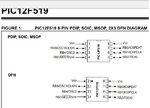
12f519.jpg

I don't think it is following a specific protocol either as some part of the data don't seem to have a special standard.
 

Hi,

It is not "I2C", because I2C uses 9 clocks per byte. But in your picture there are just 8 clocks per byte.

I don't think it is following a specific protocol
You cant say if this is a "protocol" or not, as long as you don't recognize any dedicated pieces of data and frames.

Maybe you mix the phrases "interface" and "protocol".
A protocol is the language, it defines the meaning of the data.
An interface is the method, how you transport the informations. (Speaking vs writing)

With your scope pictures you may find out what "interface" it is, but it will be hard to find out what protocol it is:
From the pictures you see:
* it is two wire
* it is synchronous
* it is 8 clocks per byte
* a data line
* a clock line
* the timing when "data" is pushed on the line with respect to clock
* the voltage levels
(It may be USART or SPI...)

But you don't (easily) see protocol related specifications like:
* whether the data and clock channels are bidirectional
* if the idle timing is a part of the protocol
* the meaning of each byte
...

Klaus
 
The 12F519 is one of the most basic PICs ever made and is does not have a USART or SPI module on-board so whatever makes and recognizes these signals is doing it in software. I agree it 'looks' like synchronous serial but it is almost impossible to implement that in software without a serial clock signal as well. A digital PLL for data recovery in less than 1K of program space and 41 bytes of RAM would be quite an achievement!

Saeedazari, can you tell us which pins are used on the PICs please. GP3 (pin 4) is an input only pin so if it is being used, it might give some clue about the data.

Brian.
 

Thanks for your reply.
Pin 6 & 7 are being used on the PCB. PIN 6 is RB1/ICSPCLK and PIN 7 is RB0/ICSPDAT.
The PIC does not have a lot of data to send to the mainboard. Maybe just some numbers and after that, mainboard does not need the PIC anymore.
 

What data sheet are you using for the PIC12F519?
The one on the Microchip web site is https://ww1.microchip.com/downloads/en/DeviceDoc/41319B.pdf and it does not refer to the I/O pins as 'RBx' - instead it uses the 'GPx' nomenclature.
(Not that it really matters in this case - they seem to refer to the same pins.)
Can you tell us what else is connected to the PIC? IT might give some clue as to what the "numbers" being sent are.
Also, when you say the main board does not need the PIC after it has sent the "numbers", what triggers the PIC to send the numbers in the first place? Are the numbers sent again - if so after how long?
Susan
 

Another thing: can you tell which is the source of the signals? I'm getting the impression this might be a 'dongle' to unlock something. If that's the case, one signal might be from the mainboard and the other a response from the PIC.

Brian.
 
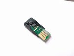
Yes it is a dongle to unlock a unit. Here is the the picture:
pic12f519.jpg

If so, the CPU is just sending clock signals?
 

As a security device it almost certainly doesn't use any standard protocol. I would guess, and that is all I can do without seeing the whole system, it works like this:

1. something on the main board resets the dongle. This could be by power cycling it or by sending it some special sequence of pulses.
2. After reset, the dongle waits for a sequence of clock pulses from the main board.
3. at each clock pulse, the dongle sets or resets it's output pin to send a code back to the main board.

It is possible it sends a different code back each time, you should run the logic analyzer several times to see if it repeats the same pulse pattern.

Brian.
 
Status
Not open for further replies.

Similar threads

Part and Inventory Search

Welcome to EDABoard.com

Sponsor

Back
Top