Continue to Site

Welcome to EDAboard.com

Welcome to our site! EDAboard.com is an international Electronics Discussion Forum focused on EDA software, circuits, schematics, books, theory, papers, asic, pld, 8051, DSP, Network, RF, Analog Design, PCB, Service Manuals... and a whole lot more! To participate you need to register. Registration is free. Click here to register now.

[SOLVED] How can I calculate the (W/L) ratio for nmos and pmos in below schematics?

Status
Not open for further replies.

viny9694

Newbie level 2
Joined
Jul 9, 2018
Messages
2
Helped
0
Reputation
0
Reaction score
0
Trophy points
1
Activity points
15
Hi all,

I'm designing a D flip flop cadence virtuoso 180nm Technology. First, I designed the schematic with 1u/500nm for pmos/nmos (I took randomly), then I performed the simulation. But, getting the output in mV instead of V for 1.8V source. Does size matters? I f so how can I calculate for the below schematics?
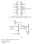
1.PNG

2.PNG

Thank you.
 

I see no 1.8V source in either schematic, neither of which look
like they are "live" CAD simulation schematics.

If you use uniform W/L then you will not see things work right.
For example the "bus hold" double inverter in the upper pic
will never be overcome by the solo PMOS (vs stronger BH
NMOS) or the double stack NMOS (vs stronger single PMOS
in inverter). So the information on that "X" node may have
only "contention" and "failed" as its logic states.

Similarly half-latch-TINV-based DFFs require that the
feedback be weaker than the forward path to get decent
setup time (or even plain functionality). NAND / NOR
based DFFs do not have this issue, only slowness and
bloat.

"One Size Does Not Fit All" is, I think, today's lesson. But
do not neglect the 1.8V supply's explicit voltage source.
 

Status
Not open for further replies.

Part and Inventory Search

Welcome to EDABoard.com

Sponsor

Back
Top