adeniyiMokesioluwa
Newbie level 4
Good day, All
I am drawing the layout of an LNA using 130 nm GF SiGe BiCMOS process in ADS Keysight. However, I have some issues with it.
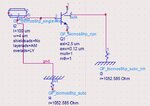
1. The HBT transistor is composed of 4 terminal, the 4th being the bulk terminal (connection to substrate). In the schematic, it is connected to the "in" terminal of the substrate. However, the 4th terminal is missing on the layout. My LVS therefore has been failing because of the absence of this connection.
How can i connect this on the layout?.
2. My single wire transmission line also has 3 terminal, the third being labelled the "vshield" which must be connected to a pure AC ground. This I was able to connect successfully on the schematic but on the layout, the "vshield" is missing. I have looked at the training material , where it was recommended that the substrate be position at least 80 um aaway from the transmission line. However, my LVS still fails.
How can i resolve this?
Thanks for your suggestion and response.
[/LIST]

